
|
|
[China]

Trade Verify
Address: Rm5-616,No.851,Dianshanhu avenue, Qingpu area,Shanghai city,CHINA
Contact name:Wang

SHANGHAI FAMOUS TRADE CO.,LTD |
|
Verified Suppliers
|
|
|
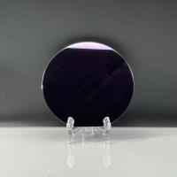
4'' 200nm AlScN Template On Silicon SSP DSP Epitaxial Substrates for LED Devices
Features:
Aluminum scandium nitride (AlScN) on silicon refers to the deposition of a thin AlScN on a silicon substrate. This process involves growing a layer of AlScN material on the surface of a sapphire wafer using techniques such as molecular beam epitaxy (MBE) or metal-organic chemical vapor deposition (MOCVD). Aluminum scandium nitride (AlScN) is a a wide-band gap semiconductor material composed of aluminum (Al), scandium (Sc), and nitrogen (N). Due to its excellent piezoelectric and acoustic properties, it is an ideal material for high-frequency acoustic devices. It is considered as the most promising substrate for 5G radio frequency SAW/BAW filters.


Specification:
Related Product:


Company Introduction:
SHANGHAI FAMOUS TRADE CO.,LTD. locates in the city of Shanghai, Which is the best city of China, and our factory is founded in Wuxi city in 2014.We specialize in processing a varity of materials into wafers, substrates and custiomized optical glass parts.components widely used in electronics, optics, optoelectronics and many other fields. We also have been working closely with many domestic and oversea universities, research institutions and companies, provide customized products and services for their R&D projects. It's our vision to maintaining a good relationship of cooperation with our all customers by our good reputatiaons.

FAQ:
Q: What's your MOQ?
A: (1) For inventory, the MOQ is 1pcs.
(2) For customized products, the MOQ is 5pcs up.
Q: What's the way of shipping and cost?
A:(1) We accept DHL, Fedex, EMS etc.
(2) If you have your own express account, it's great.If not,we could help you ship them.
Freight is in accordance with the actual settlement.
Q: What's the delivery time?
For inventory: the delivery is 5 workdays after you place the order.
For customized products: the delivery is 2 or 3 weeks after you place the order.
Q: Do you have standard products?
A: Our standard products in stock.as like 4inch 0.65mm,0.5mm polished wafer.
Q: How to pay?
A:50%deposit, left before delivery T/T,
Q: Can I customize the products based on my need?
A: Yes, we can customize the material, specifications and optical coating for your optical
components based on your needs.


