|
|
[China]

Trade Verify
Address: Rm5-616,No.851,Dianshanhu avenue, Qingpu area,Shanghai city,CHINA
Contact name:Wang

SHANGHAI FAMOUS TRADE CO.,LTD |
|
Verified Suppliers
|
|
|
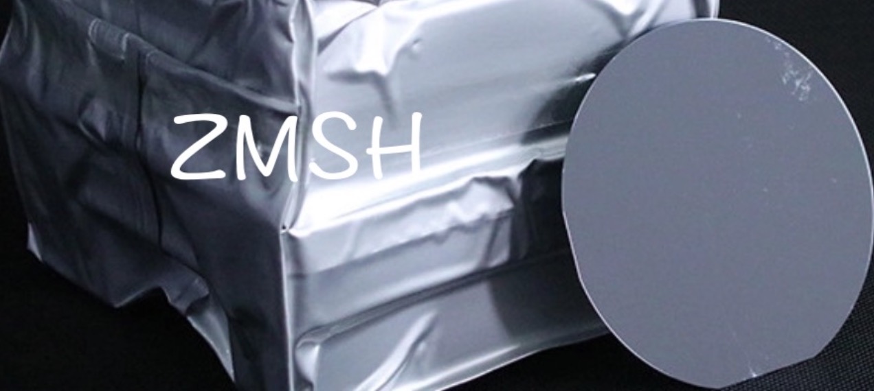
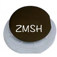
2'' 4'' InP Wafer Indium Phosphide Wafer Semiconductor Substrates 350um 650um
Description of InP wafer:
InP (Indium phosphide) chips are a commonly used semiconductor material for the manufacture of high-performance optoelectronic devices such as photodiodes, lasers and photoelectric sensors.
Features of InP wafer:
InP (Indium phosphide) chip is widely used in the field of optoelectronic devices as the substrate material of semiconductor devices. Here are some of the advantages of InP chip substrate materials:
Technical Parameters of InP wafer:
| Item | Parameter | UOM |
| Material | InP | |
| Conduction type/Dopant | S-C-N/S | |
| Grade | Dummy | |
| Diameter | 100.0+/-0.3 | mm |
| Orientation | (100) +/-0.5° | |
| Lamellar twin area | useful single crystal area with (100) orienation > 80% | |
| Primary Flat Orientation | EJ(0-1-1) | mm |
| Primary Flat Length | 32.5+/-1 | |
| Secondary Flat Orientation | EJ(0-11) | |
| Secondary Flat Length | 18+/-1 |
Applications of InP wafer:
InP (Indium phosphide) chip, as the substrate material of semiconductor devices, has excellent photoelectric and electrical properties. The following are some of the main application areas of InP chip substrate materials:

FAQ:
Q1: What brand name is the InP wafer?
A1: The Indium Phosphide is made by ZMSH.
Q2: What's the diameter of the Indium Phosphide?
A2: Thediameter of Indium Phosphide is 2'', 3'', 4''.
Q3: Where is the Indium Phosphide from?
A3: The Indium Phosphide is from China.
Q4: Is the Indium Phosphide ROHS certified?
A4: Yes, the Indium Phosphide is ROHS certified.
Q5: How many Indium Phosphide wafes can I buy at 1 time?
A5: The minimum order quantity of the Indium Phosphide is 5pcs.
Other products: