
|
|
[China]

Trade Verify
Address: Rm5-616,No.851,Dianshanhu avenue, Qingpu area,Shanghai city,CHINA
Contact name:Wang

SHANGHAI FAMOUS TRADE CO.,LTD |
|
Verified Suppliers
|

|
|
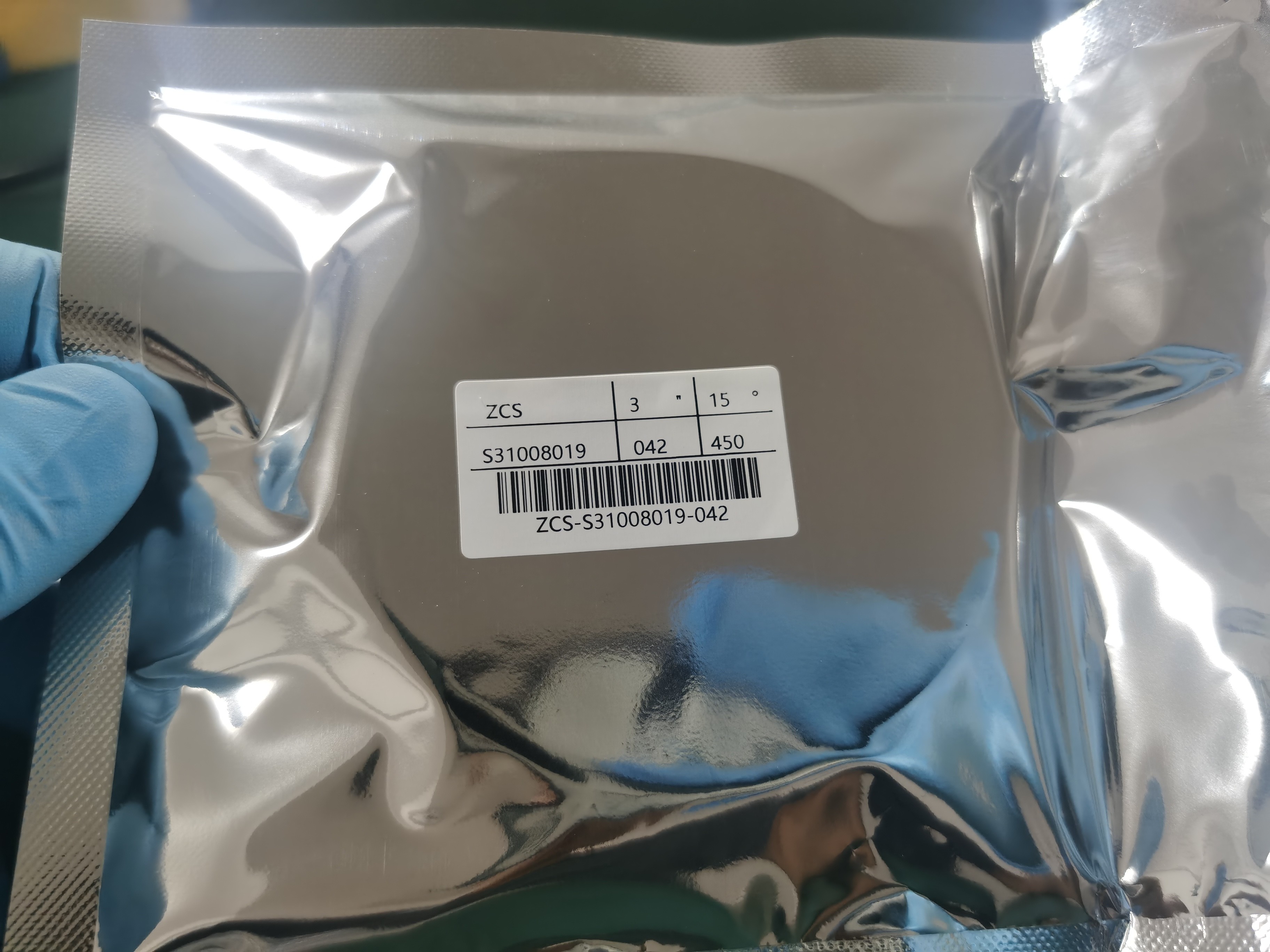
6inch VGF Growth Method P Type GaAs Wafers GaAs Substrates
------------------------------------------------------------------------------------------------------------------------------
GaAs wafer
GaAs Wafers GaAs Substrate Wafers GaAS substrate wafers GaAS is a semiconductor material with superior properties of high frequency, high electron migration, high electron performance, low salivary sound and linear goodness. It is widely used in the optoelectronics and microelectronics industries. In the optoelectronics industry, GaAS substrate wafers can be used for manufacturing LED(light emitting tube), LD(teaching light garden), photovoltaic devices, etc. In the field of microelectronics industry, it can be used to make MESFET(metal semiconductor field effect leather tube), HEMT(high electron mobility transistor),HBT(heterojunction bipolar transistor),IC, microwave diode,Hall device, etc.
| GaAs (Gallium Arsenide) for LED Applications | ||
| Item | Specifications | Remarks |
| Conduction Type | SC/n-type | |
| Growth Method | VGF | |
| Dopant | Silicon | |
| Wafer Diamter | 2, 3 & 4 inch | Ingot or as-cut available |
| Crystal Orientation | (100)2°/6°/15° off (110) | Other misorientation available |
| OF | EJ or US | |
| Carrier Concentration | (0.4~2.5)E18/cm3 | |
| Resistivity at RT | (1.5~9)E-3 Ohm.cm | |
| Mobility | 1500~3000 cm2/V.sec | |
| Etch Pit Density | <500/cm2 | |
| Laser Marking | upon request | |
| Surface Finish | P/E or P/P | |
| Thickness | 220~350um | |
| Epitaxy Ready | Yes | |
| Package | Single wafer container or cassette | |
Product display

ABOUT OUR ZMKJ


Q: What's the MOQ?
(1) For inventory, the MOQ is 5pcs.
(2) For customized products, the MOQ is 10pcs-30pcs.
Q: Do you have inspection report for material?
We can supply detail report for our products.


