| Specification | A62.4500 | A622.4501 | A62.4503 | A62.4505 |
| Work Mode | Tapping Mode
【Optional】
Contact Mode
Friction Mode
Phase Mode
Magnetic Mode
Electrostatic Mode | Contact Mode
Tapping Mode
【Optional】
Friction Mode
Phase Mode
Magnetic Mode
Electrostatic Mode | Contact Mode
Tapping Mode
【Optional】
Friction Mode
Phase Mode
Magnetic Mode
Electrostatic Mode | Contact Mode
Tapping Mode
【Optional】
Friction Mode
Phase Mode
Magnetic Mode
Electrostatic Mode |
| Current Spectrum Curve | RMS-Z Curve
【Optional】
F-Z Force Curve | RMS-Z Curve
F-Z Force Curve | RMS-Z Curve
F-Z Force Curve | RMS-Z Curve
F-Z Force Curve |
| XY Scan Range | 20×20um | 20×20um | 50×50um | 50×50um |
| XY Scan Resolution | 0.2nm | 0.2nm | 0.2nm | 0.2nm |
| Z Scan Range | 2.5um | 2.5um | 5um | 5um |
| Y Scan Resolution | 0.05nm | 0.05nm | 0.05nm | 0.05nm |
| Scan Speed | 0.6Hz~30Hz | 0.6Hz~30Hz | 0.6Hz~30Hz | 0.6Hz~30Hz |
| Scan Angle | 0~360° | 0~360° | 0~360° | 0~360° |
| Sample Size | Φ≤90mm
H≤20mm | Φ≤90mm
H≤20mm | Φ≤90mm
H≤20mm | Φ≤90mm
H≤20mm |
| XY Stage Moving | 15×15mm | 15×15mm | 25×25um | 25×25um |
| Shock-Absorbing Design | Spring Suspension | Spring Suspension
Metal Shielding Box | Spring Suspension
Metal Shielding Box | - |
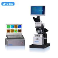
| Optical Syestem | 4x Objective
Resolution 2.5um | 4x Objective
Resolution 2.5um | 10x Objective
Resolution 1um | Eyepiece 10x
Infinity Plan LWD APO 5x10x20x50x
5.0M Digital Camera
10" LCD Monitor, With Measuring
LED Kohler Illumination
Coaxial Coarse & Fine Focusing |
| Output | USB2.0/3.0 | USB2.0/3.0 | USB2.0/3.0 | USB2.0/3.0 |
| Software | Win XP/7/8/10 | Win XP/7/8/10 | Win XP/7/8/10 | Win XP/7/8/10 |