Structure of FPC
According to the number of layers of conductive copper foil, FPC
can be divided into single layer circuit, double layer circuit,
multi-layer circuit, double sided and so on.
Single-layer structure: the flexible circuit of this structure is
the simplest structure of the flexible PCB. Usually the base
material (dielectric substrates) + transparent rubber(adhesive) +
copper foil is a set of purchased raw materials(semi-manufactures),
the protective film and transparent glue are another kind of bought
raw material. First, copper foil must be etched to obtain the
required circuit, and the protective film should be drilled to
reveal the corresponding pad. After cleaning, the two are combined
by rolling. Then the exposed part of the pad electroplated gold or
tin to protect. In this way, the big panel board will be ready.
Generally also it’s stamped into the corresponding shape of the
small circuit board. There is also no protective film directly on
the copper foil, but printed resistance soldering coating, so that
the cost will be lower, but the mechanical strength of the circuit
board will become worse. Unless the strength requirement is not
high and the price needs to be as low as possible, it is best to
apply the protective film method.
Double layer structure: when the circuit is too complex to be
wired, or copper foil is needed to shield the ground, it is
necessary to choose a double layer or even a multilayer. The most
typical difference between a multilayer and a single plate is the
addition of a perforated structure to connect the layers of copper
foil. The first process of transparent rubber + base material +
copper foil is to make holes. Drill holes in the base material and
copper foil first, clean and then plated with a certain thickness
of copper. The subsequent fabrication process is almost the same as
the single-layer circuit.
Double sided structure: both sides of the double sided FPC have
pads, mainly used to connect other circuit boards. Although it and
monolayer structure is similar, but the manufacturing process is
very different. Its raw material is copper foil, protective film
and transparent glue. The protective film should be drilled
according to the position of the pad first, then the copper foil
should be affixed, the pad and track lines should be etched and
then the protective film of another drilled hole should be affixed.
Copper foil is available in two different types of copper: ED
Copper and RA copper.
ED copper is an electro-deposited (ED) copper foil produced in the
same way as the copper foil used for rigid printed circuit boards.
This also means that the copper is “treated”, i.e., it has a
slightly rough surface on one side, which ensures a better adhesion
when the copper foil is bonded to the base material.
RA copper is a rolled and annealed copper foil produced from
electrolytically deposited cathode copper, which is melted and cast
into ingots. The ingots are first hot-rolled to a certain size and
milled on all surfaces. The copper is then cold-rolled and
annealed, until the desired thickness is obtained.
Copper foil is available in thickness of 12, 18, 35 and 70 μm.
The most common available for dielectric substrate and coverlay is
polyimide films. This material can also be used as coverlay.
Polyimide is best suited for flexible circuits because of its
characteristics as stated below:
High temperature resistance allows soldering operations without
damaging the flexible circuits
Very good electrical properties
Good chemical resistance
Polyimide is available in thicknesses of 12.5, 20, 25 and 50 μm.
Base laminates for rigid printed circuit boards are copper foils
laminated together with the base materials, the adhesive coming
from the prepreg material during lamination. Contrary to this is
the flexible circuit where the lamination of the copper foil to the
film material is achieved by means of an adhesive system. It is
necessary to distinguish between two main systems of adhesive,
namely thermoplastic and thermoset adhesives. The choice is
dictated partly by the processing, and partly by the application of
the finished flexible circuit.
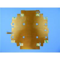
FPC Case: Double Sided Flexible PCB board With 0.15mm thick and
Immersion Gold
(FPC’s are custom-made products, the picture and parameters shown
are just for reference)
General description
This is a type of flexible printed circuit for the application of
GPS tracking systems. It’s a 2 layer board at 0.15mm thick. The
base laminate is from ITEQ, It’s fabricated per IPC 6012 Class 2
using supplied Gerber data. Polyimide stiffener is applied on the
inserting part.
Parameter and data sheet
| Number of Layers | 2 |
| Board Size | 160 x 165mm=1PCS |
| Board Type | Flexbile cirucit |
| Board Thickness | 0.15mm +/-10% |
| Board Material | Polyimide (PI) 25um |
| Board Material Supplier | ITEQ |
| Tg Value of Board Material | 60℃ |
| |
| PTH Cu thickness | ≥20 um |
| Inner Iayer Cu thicknes | N/A |
| Surface Cu thickness | 35 um (1oz) |
| |
| Coverlay Colour | Yellow |
| Number of Coverlay | 2 |
| Thickness of Coverlay | 25 um |
| Stiffener | NO |
| |
| Type of Silkscreen Ink | NO |
| Supplier of Silkscreen | NO |
| Color of Silkscreen | NO |
| Number of Silkscreen | NO |
| |
| Mininum Trace (mil) | 4 mil |
| Minimum Gap(mil) | 4 mil |
| |
| Surface Finish | Immersion Gold |
| RoHS Required | Yes |
| Famability | 94-V0 |
| |
| Thermal Shock Test | Pass, -25℃±125℃, 1000 cycles. |
| Thermal Stress | Pass, 300±5℃,10 seconds, 3 cycles. No delamination, no blistering. |
| Function | 100% Pass electrical test |
| Workmanship | Compliance with IPC-A-600H & IPC-6013C Class 2 |
Features and benefits
Excellent flexibility
Reducing the volume
Weight reduction
Consistency of assembly
Increased reliability
Controllability of electrical parameter design
The end can be whole soldered
Material optionality
Low cost
Continuity of processing
Quick and on-time delivery
Make delivery on time. We keep higher than 98% on-time-delivery
rate.
Application
Keypad FPC, Industrial control computer soft board, consumer ETC
(Electronic Toll Collection ) soft board,
About Us
Bicheng PCB, a unique printed circuit board supplier based in
Shenzhen China serves worldwide customers since it’s born in 2003.
At Bicheng, every batch of PCB goes through electrical test, AOI
inspection, high voltage test, Impedance control test,
micro-section, solder-ability test, thermal stress test,
reliability test, insulation resistance test and ionic
contamination test etc. Finally it is like a beautiful gift to be
delivered to your hands.
Different plant scale to suit for your requirements
16000 square meter factory building
30000 square meter month capability
8000 types of PCB per month
ISO9001, ISO14001, TS16949, UL Certified
Variety of PCB technology to meet the market demands
HDI board
Heavy copper board
Hybrid material board
Blind via board
High frequency board
Metal core board
Immersion gold board
Multilayer board
Backplane board
Gold finger board
Comprehensive sales service presale, in sale and after sale.
Quick CADCAM checking and free PCB quotation
Free-of-charge PCB panelization
Prototype PCB capability
Volume Production capability
Quick turn-around samples
Free-of-charge PCB test
Solid carton packing