Home Companies Shenzhen Bicheng Electronics Technology Co., Ltd

RT/duroid 6035HTC PCB DK3.5 at 10 GHz 30mil double layer 1oz copper with Immersion Silver

Shenzhen Bicheng Electronics Technology Co., Ltd
Active Member

Contact Us

[China] country

Address: 6-11C Shidai Jingyuan Fuyong Town, Baoan District, Shenzhen City, Guangdong Province, China

Contact name:Sally Mao

Inquir Now

Shenzhen Bicheng Electronics Technology Co., Ltd

RT/duroid 6035HTC PCB DK3.5 at 10 GHz 30mil double layer 1oz copper with Immersion Silver

Country/Region china
City & Province shenzhen guangdong
Categories Solar Chargers
InquireNow

Product Details

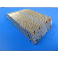
Raise the Bar with Our New High-Power RF PCB


Engineers searching for the ultimate PCB foundation for microwave and RF designs, look no further! We're thrilled to announce the launch of our new high-performance rigid board that takes RF circuit design to the next level.


Built on Rogers' acclaimed RT/duroid 6035HTC material, this board boasts best-in-class thermal management and electrical performance. The ceramic-filled PTFE composite substrate has excellent dielectric properties, with a low and stable loss tangent for minimal signal loss up to 10GHz. And the high thermal conductivity rapidly dissipates heat from high power components.


Stackup & Materials

  • Substrate: Rogers RT/duroid 6035HTC, 0.762mm (30 mil) thickness. Dielectric constant of 3.5 at 10 GHz. Extremely low loss (Df of 0.0013 at 10 GHz) and thermal coefficient of Dk of -66 ppm/°C. Operational range of -40°C to +85°C.
  • Copper Foil: Electrodeposited rolled annealed copper, 35 μm thickness on both layers, with thermally stable reverse treat for optimal high frequency signal integrity.
  • Layer 1: Signal layer
  • Layer 2: Ground/power plane layer
  • Plating: 20 μm copper in holes/vias
  • Final Finished Board Thickness: 0.9mm
  • Final Copper Weight: 1 oz (1.4 mil) each outer layer


Layout Capabilities

  • Board Dimensions: 76.05mm x 53.2mm
  • Minimum Trace/Space: 6/8 mil
  • Minimum Hole Size: 0.45mm
  • All vias are thru-hole interconnects, no blind/buried vias
  • 105 vias with 20μm copper plating for robust interconnects
  • 87 components, 101 pads, supporting top and bottom SMT parts


With its reverse-treated copper layers and robust 105 vias, the PCB enables routing intricate microwave circuits with ease. The finely spaced traces and abundance of vias provide ample connectivity for complex designs. And it withstands extreme thermal cycles thanks to a thermally stable construction.


Surface Finishes

  • Immersion silver surface finish on pads and traces enables excellent solderability and thermal/electrical performance
  • No solder mask for maximum heat dissipation
  • No silkscreen for simplicity


Advantages:

  • Excellent high frequency performance - The Rogers RT/duroid 6035HTC dielectric material has a low loss tangent, stable dielectric constant, and low thermal coefficient of Dk for reliable performance up to 10GHz.
  • High thermal conductivity - The ceramic-filled PTFE composite material dissipates heat efficiently, enabling operation at higher power levels.
  • Thermally stable construction - The reverse treat copper foil minimizes thermal expansion issues over wide temperature swings.
  • High density routing capabilities - With 6/8 mil trace/space, dense RF layouts can be achieved.
  • Abundant vias - 105 vias with 20μm copper plating provide robust interconnects between layers.
  • Lead-free immersion silver finish - Provides excellent solderability and thermal/electrical conduction from pads.
  • No solder mask - Allows for maximum heat dissipation across board surface.
  • 100% electrical testing - Ensures quality and reliability.


We designed this board to be the ultimate microwave PCB platform. Ideal for high frequency analog and digital, microwave, and mm-Wave applications. Integrate it into your designs to reach new levels of performance.


Of course, these advanced capabilities come at a cost. The specialized materials and fabrication result in a higher price tag compared to standard PCBs. And the 2-layer stackup limits routing flexibility versus a 4+ layer board. But for RF/microwave products where electrical performance and thermal management are vital, the benefits outweigh the costs.


Disadvantages:

  • Higher cost - The advanced dielectric material and fabrication is more expensive than standard FR-4 PCBs.
  • Limited layer count - The 2-layer construction reduces routing flexibility compared to a 4+ layer board.
  • No solder mask - Lack of solder mask may require extra handling and cleaning precautions.
  • Limited board sizes - Currently only available in one fixed dimension of 76.05mm x 53.2mm.
  • No blind/buried vias - Thru-hole vias take up more routing space versus blind/buried vias.
  • Lead time - Advanced PCBs typically have longer fabrication lead times.


Should you have any technical inquiries or require further assistance, please do not hesitate to contact Sally Mao at sales30@bichengpcb.com. Our dedicated team stands ready to address any questions or concerns you may encounter. We can't wait to see the leading-edge innovations you create with this new RF board!

Hot Products

Rogers RF and Microwave PCB on 60mil 1.524mm AD250C Substrates With Immersion Gold (Printed Circuit ...
DiClad 870 Microwave PCB with HASL Double Sided 31mil 0.8mm Thick no Solder Maks no Silkscreen ...
Rogers DiClad 870 Woven Fiberglass Reinforced PTFE-based 31mil 93mil 125mil Microwave PCB (Printed ...
Rogers CLTE-XT High Frequency PCB 9.4mil 25mil 40mil 59mil ceramic filled woven glass reinforced ...
PCB with Peelable Mask Double Sided Circuit Board Built on Tg170 FR-4 Coating HASL. (Printed ...
Edge Castellated PCB Half Holes Circuit Boards Built On 1.6mm FR-4 With Blue Solder Mask (Printed ...