

Active Member
|
[China]

Address: Room 36B1-B2, Building C, Electronics Science & Technology Building Shennan Mid-Road, Shenzhen China
Contact name:Sharon Yang

Anterwell Technology Ltd. |
|
|
HT48R05A-1 8-Bit OTP Microcontroller
Features
General Description
The device is an 8-bit high performance RISC-like microcontroller designed for multiple I/O product applications. The device is particularly suitable for use in products such as remote controllers, fan/light controllers, washing machine controllers, scales, toys and various subsystem controllers. A halt feature is included to reduce power consumption. The program and option memories can be electrically programmed, making the microcontroller suitable for use in product development.
Absolute Maximum Ratings
Supply Voltage ...............VSS-0.3V to VSS+5.5V
Storage Temperature.................-50℃ to 125℃
Input Voltage.................VSS-0.3V to VDD+0.3V
Operating Temperature ..............-40℃ to 85℃
Note: These are stress ratings only. Stresses exceeding the range specified under "Absolute Maximum Ratings" may cause substantial damage to the device. Functional operation of this device at other conditions beyond those listed in the specification is not implied and prolonged exposure to extreme conditions may affect device reliability.
Functional Description
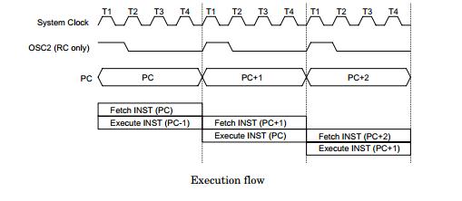
Execution flow
The system clock for the microcontroller is derived from either a crystal or an RC oscillator. The system clock is internally divided into four non-overlapping clocks. One instruction cycle consists of four system clock cycles.
Instruction fetching and execution are pipelined in such a way that a fetch takes an instruction cycle while decoding and execution takes the next instruction cycle. However, the pipelining scheme causes each instruction to effectively execute in a cycle. If an instruction changes the program counter, two cycles are required to complete the instruction.
Program counter--PC
The program counter (PC) controls the sequence in which the instructions stored in program PROM are executed and its contents specify full range of program memory.
After accessing a program memory word to fetch an instruction code, the contents of the program counter are incremented by one. The program counter then points to the memory word containing the next instruction code.
When executing a jump instruction, conditional skip execution, loading PCL register, subroutine call, initial reset, internal interrupt, external interrupt or return from subroutine, the PC manipulates the program transfer by loading the address corresponding to each instruction.
The conditional skip is activated by instructions. Once the condition is met, the next instruction, fetched during the current instruction execution, is discarded and a dummy cycle replaces it to get the proper instruction. Otherwise proceed with the next instruction.
The lower byte of the program counter (PCL) is a readable and writable register (06H). Moving data into the PCL performs a short jump. The destination will be within 256 locations.
When a control transfer takes place, an additional dummy cycle is required.
Program memory--PROM
The program memory is used to store the program instructions which are to be executed. It also contains data, table, and interrupt entries, and is organized into 51214 bits, addressed by the program counter and table pointer.
Block Diagram

Pin Assignment


