

Active Member
|
[China]

Address: Room 36B1-B2, Building C, Electronics Science & Technology Building Shennan Mid-Road, Shenzhen China
Contact name:Sharon Yang

Anterwell Technology Ltd. |

|
|
Single-chip 16/32-bit microcontrollers; 32/64/128/256/512 kB ISP/IAP Flash with 10-bit ADC and DAC
General description
The LPC2131/2132/2134/2136/2138 microcontrollers are based on a 32/16 bit ARM7TDMI-S CPU with real-time emulation and embedded trace support, that combines the microcontroller with 32 kB, 64 kB, 128 kB, 256 kB and 512 kB of embedded high speed Flash memory. A 128-bit wide memory interface and a unique accelerator architecture enable 32-bit code execution at maximum clock rate. For critical code size applications, the alternative 16-bit Thumb mode reduces code by more than 30 % with minimal performance penalty.
Due to their tiny size and low power consumption, these microcontrollers are ideal for applications where miniaturization is a key requirement, such as access control and point-of-sale. With a wide range of serial communications interfaces and on-chip SRAM options of 8/16/32 kB, they are very well suited for communication gateways and protocol converters, soft modems, voice recognition and low end imaging, providing both large buffer size and high processing power. Various 32-bit timers, single or dual 10-bit 8 channel ADC(s), 10-bit DAC, PWM channels and 47 GPIO lines with up to nine edge or level sensitive external interrupt pins make these microcontrollers particularly suitable for industrial control and medical systems.
Key features
■ 16/32-bit ARM7TDMI-S microcontroller in a tiny LQFP64 package.
■ 8/16/32 kB of on-chip static RAM and 32/64/128/256/512 kB of on-chip Flash program memory. 128 bit wide interface/accelerator enables high speed 60 MHz operation.
■ In-System/In-Application Programming (ISP/IAP) via on-chip boot-loader software. Single Flash sector or full chip erase in 400 ms and programming of 256 bytes in 1 ms.
■ EmbeddedICE RT and Embedded Trace interfaces offer real-time debugging with the on-chip RealMonitor software and high speed tracing of instruction execution.
■ One (LPC2131/32) or two (LPC2134/36/38) 8 channel 10-bit A/D converters provides a total of up to 16 analog inputs, with conversion times as low as 2.44 µs per channel.
■ Single 10-bit D/A converter provides variable analog output (LPC2132/34/36/38).
■ Two 32-bit timers/external event counters (with four capture and four compare channels each), PWM unit (six outputs) and watchdog.
■ Low power Real-time clock with independent power and dedicated 32 kHz clock input.
■ Multiple serial interfaces including two UARTs (16C550), two Fast I2C-bus (400 kbit/s), SPI and SSP with buffering and variable data length capabilities.
■ Vectored interrupt controller with configurable priorities and vector addresses.
■ Up to 47 5 V tolerant general purpose I/O pins in tiny LQFP64 package.
■ Up to nine edge or level sensitive external interrupt pins available.
■ 60 MHz maximum CPU clock available from programmable on-chip PLL with settling time of 100 µs.
■ On-chip integrated oscillator operates with external crystal in range of 1 MHz to 30 MHz and with external oscillator up to 50 MHz.
■ Power saving modes include Idle and Power-down.
■ Individual enable/disable of peripheral functions as well as peripheral clock scaling down for additional power optimization.
■ Processor wake-up from Power-down mode via external interrupt or BOD.
■ Single power supply chip with POR and BOD circuits:
◆ CPU operating voltage range of 3.0 V to 3.6 V (3.3 V ± 10 %) with 5 V tolerant I/O pads.
Block diagram

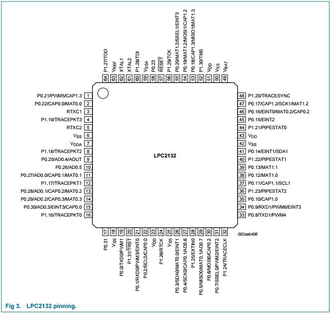
Pinning


Limiting values
In accordance with the Absolute Maximum Rating System (IEC 60134).[1]
| Symbol Parameter Conditions Min Max Unit |
| VDD supply voltage, core and external rail −0.5 +3.6 V |
| VDDA analog 3.3 V pad supply voltage −0.5 4.6 V |
| VBAT RTC power supply voltage −0.5 4.6 V |
| VREF A/D converter reference voltage −0.5 4.6 V |
| VIA analog input voltage on A/D related pins −0.5 5.1 V |
| VI DC input voltage, 5 V tolerant I/O pins [2] [3] −0.5 6.0 V |
VI DC input voltage, other I/O pins [2] −0.5 VDD + 0.5 [4] V |
| IDD DC supply current per supply pin - 100 [5] mA |
| ISS DC ground current per ground pin - 100 [5] mA |
| Tstg storage temperature [6] −40 125 °C |
Ptot(pack) total power dissipation based on package - 1.5 W heat transfer, not device power consumption |
[1] The following applies to the Limiting values:
a) Stresses above those listed under Limiting values may cause permanent damage to the device. This is a stress rating only and functional operation of the device at these or any conditions other than those described in Section 8 “Static characteristics”and Section 9 “Dynamic characteristics” of this specification is not implied.
b) This product includes circuitry specifically designed for the protection of its internal devices from the damaging effects of excessive static charge. Nonetheless, it is suggested that conventional precautions be taken to avoid applying greater than the rated maximum.
c) Parameters are valid over operating temperature range unless otherwise specified. All voltages are with respect to VSS unless otherwise noted.
[2] Including voltage on outputs in 3-state mode.
[3] Only valid when the VDD supply voltage is present.
[4] Not to exceed 4.6 V.
[5] The peak current is limited to 25 times the corresponding maximum current.
[6] Dependent on package type.
Package outline
LQFP64: plastic low profile quad flat package; 64 leads; body 10 x 10 x 1.4 mm SOT314-2

Fig 5. Package outline SOT314-2 (LQFP64).


