Active Member
|
[China]

Address: Room 36B1-B2, Building C, Electronics Science & Technology Building Shennan Mid-Road, Shenzhen China
Contact name:Sharon Yang

Anterwell Technology Ltd. |

|
|
TOSHIBA Field Effect Transistor
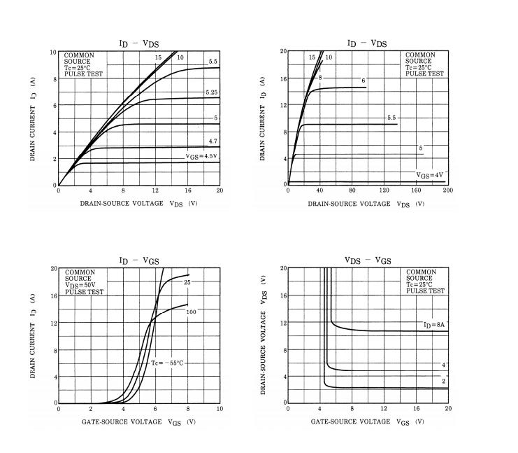
Silicon N Channel MOS Type (π−MOSIII) 2SK2611
DC−DC Converter, Relay Drive and Motor Drive Applications
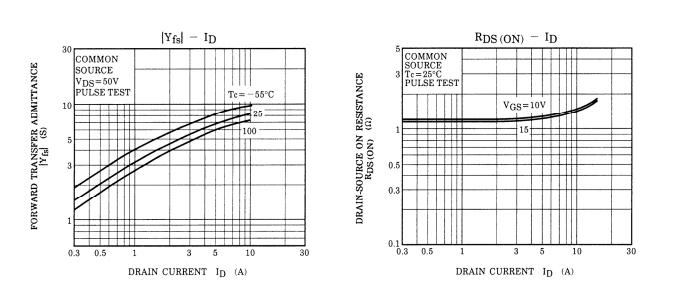
* Low drain−source ON resistance : RDS (ON) = 1.1 Ω (typ.)
* High forward transfer admittance : |Yfs| = 7.0 S (typ.)
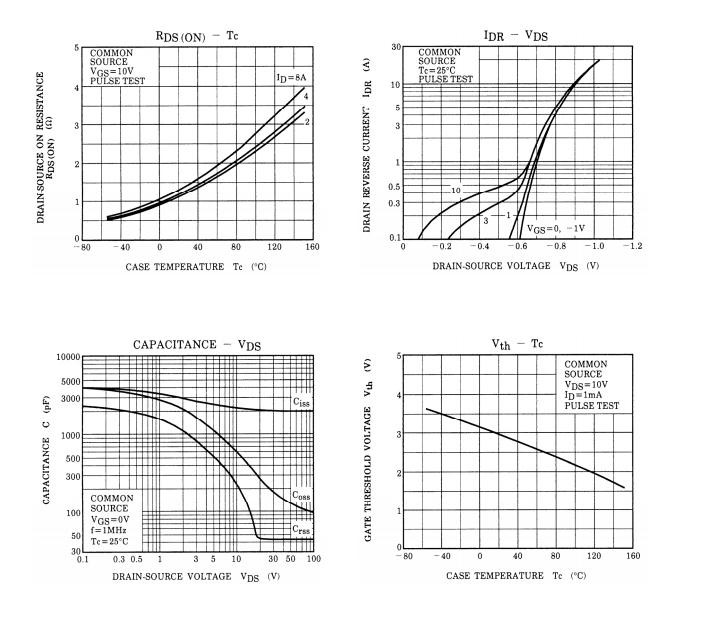
* Low leakage current : IDSS = 100 μA (max) (VDS = 720 V)
* Enhancement−mode : Vth = 2.0~4.0 V (VDS = 10 V, ID = 1 mA)
Weight: 4.6 g (typ.)
Absolute Maximum Ratings (Ta = 25°C)
| Characteristics | Symbol | Rating | Unit | |
| Drain−source voltage | VDSS | 900 | V | |
| Drain−gate voltage (RGS = 20 kΩ) | VDGR | 900 | V | |
| Gate−source voltage | VGSS | ±30 | V | |
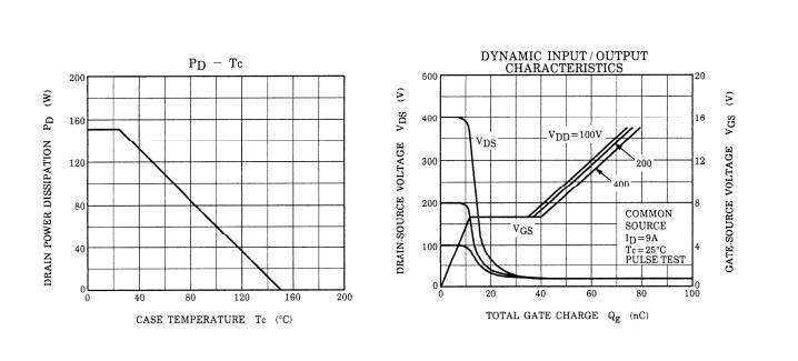
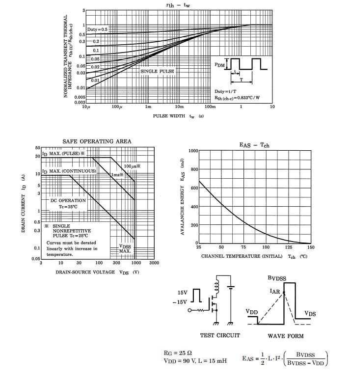
| Drain current | DC (Note 1) | ID | 9 | A |
| Pulse (Note 1) | IDP | 27 | A | |
| Drain power dissipation (Tc = 25°C) | PD | 150 | W | |
| Single pulse avalanche energy (Note 2) | EAS | 663 | mJ | |
| Avalanche current | IAR | 9 | A | |
| Repetitive avalanche energy (Note 3) | EAR | 15 | mJ | |
| Channel temperature | Tch | 150 | °C | |
| Storage temperature range | Tstg | −55~150 | °C | |
Note: Using continuously under heavy loads (e.g. the application of high temperature/current/voltage and the significant change in temperature, etc.) may cause this product to decrease in the reliability significantly even if the operating conditions (i.e. operating temperature/current/voltage, etc.) are within the absolute maximum ratings. Please design the appropriate reliability upon reviewing the Toshiba Semiconductor Reliability Handbook (“Handling Precautions”/Derating Concept and Methods) and individual reliability data (i.e. reliability test report and estimated failure rate, etc).
Thermal Characteristics
| Characteristics | Symbol | Max | Unit |
| Thermal resistance, channel to case | Rth (ch−c) | 0.833 | °C / W |
| Thermal resistance, channel to ambient | Rth (ch−a) | 50 | °C / W |
Note 1: Please use devices on condition that the channel temperature is below 150°C.
Note 2: VDD = 90 V, Tch = 25°C (initial), L = 15 mH, RG = 25 Ω, IAR = 9 A
Note 3: Repetitive rating: Pulse width limited by maximum channel temperature
This transistor is an electrostatic sensitive device.
Please handle with caution.
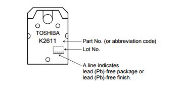
Marking