

Active Member
|
[China]

Address: Block 4, No. 5, Torch Ave, Jiulongpo District, Chongqing,400080 China
Contact name:Lin Yue

Chongqing Newsin Technology Co., Ltd |
|
|
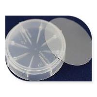
2 inch GaN Templates:
Dimensions:Ф 50.8mm ± 0.1mm
Thickness:4 µm, 20 µm; 4 µm
Orientation:C-plane(0001) ± 0.5°
Conduction Type:N-type(Undoped); N-type(Si-doped); P-type(Mg-doped)
Resistivity(300K): < 0.5 Ω·cm; < 0.05 Ω·cm; ~ 10 Ω·cm
Carrier Concentration: < 5x1017 cm-3; > 1x1018 cm-3; >
6x1016 cm-3
Mobility: ~ 300cm2/V·s; ~ 200 cm2/V·s; ~ 10 cm2/V·s
Dislocation Density: Less than 5x108 cm-2
Substrate structure: GaN on Sapphire (Standard: SSP Option: DSP)
Useable Surface Area: > 90%
4 inch GaN Templates:
Dimensions:Ф 50.8mm ± 0.1mm
Thickness: 4 µm, 20 µm; 4 µm
Orientation: C-plane(0001) ± 0.5°
Conduction Type: N-type(Undoped); N-type(Si-doped);
P-type(Mg-doped)
Resistivity(300K): < 0.5 Ω·cm; < 0.05 Ω·cm: ~ 10 Ω·cm
Carrier Concentration: < 5x1017 cm-3; > 1x1018 cm-3; >
6x1016 cm-3
Mobility: ~ 300cm2/V·s; ~ 200 cm2/V·s; ~ 10 cm2/V·s
Dislocation Density:Less than 5x108 cm-2
Substrate structure:GaN on Sapphire (Standard: SSP Option: DSP)
Useable Surface Area:> 90%
![Ceftaroline fosamil [400827-55-6]](http://img2.everychina.com/img/3c/cf/c5544c8dc1e6f52945979158b146-80x80c1-824c/ceftaroline_fosamil_400827_55_6.jpg "GaN Templates 2 & 4 inch")
![Deferasirox [201530-41-8]](http://img2.everychina.com/img/83/18/50bfb101eafcab2c17de6a46e502-80x80c1-3ac7/deferasirox_201530_41_8.jpg "GaN Templates 2 & 4 inch")
![Ezetimibe [163222-33-1]](http://img2.everychina.com/img/01/3f/10a3596178328ba2105febb135ca-80x80c1-e015/ezetimibe_163222_33_1.jpg "GaN Templates 2 & 4 inch")
![Fondaparinux sodium [114870-03-0]](http://img2.everychina.com/img/2c/0c/e47b0eaed8f897aa1a15ef2d1c81-80x80c1-c12c/fondaparinux_sodium_114870_03_0.jpg "GaN Templates 2 & 4 inch")
![Fosaprepitant dimeglumine [265121-04-8]](http://img2.everychina.com/img/6b/a6/b49897c0b87dae0e42f0ac2065d6-80x80c1-fd23/fosaprepitant_dimeglumine_265121_04_8.jpg "GaN Templates 2 & 4 inch")
![Omarigliptin (MK-3102) [1226781-44-7]](http://img2.everychina.com/img/aa/32/5f603f0cc4c42535f58c6c79e5f6-80x80c1-7f30/omarigliptin_mk_3102_1226781_44_7.jpg "GaN Templates 2 & 4 inch")