

Active Member
|
[China]

Address: 深圳市宝安区福永凤凰西区202号信诺大厦401
Contact name:吴怡

Shenzhen Yideyi Technology Limited Company |

|
|
Multilayer Printed Circuit Board Media Converter Thermometer PCBA
Shenzhen Yideyi Technology Co., Ltd founded in 2008, It's an industry leading producing and R&D manufacturer in silk screen printing, gift and electronic areas with deep domain expertise and best service to help clients get high-quality and competitive products with 13 years history. Based on our professional and innovative technologies, we produce membrane switch, flexible circuit, membrane panel, lens, crystal epoxy, adhesive sticker, name plate and so on. In addition, there is an electronic department to produce various electronic products (eg. writing tablet, air purifier, mosquito killer, keyboards, Bluetooth speaker etc).
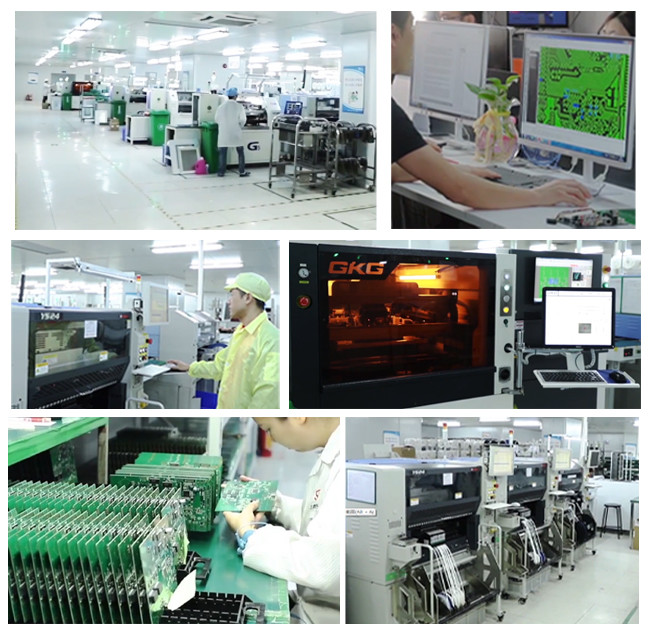
There are more than 500 staffs in our factory with a variety of
sophisticated high-end modern equipments, like all-auto silk-screen
printer, semi-auto silk screen printer (15 sets), six-color
printer, CNC engraving machine (25 sets), digital control cutting
machines, laser cutter, injection molding machine, punching
machine, etc.
We also have dust-free workshop and labs, etc. There are many
testing equipments in the labs, like binary tester,high and low
temperature tester, tension tester, height tester, membrane switch
life tester, membrane switch lead tester, etc. After several years'
development and advancement, we've gained many achievements and
certifications. Our company has passed ISO 9001:2008, ISO
14001:2004, OHSAS18001:2007, UL, SGS, TUV quality management system
certification and other related product certifications (CE, FCC,
RoHS, CCC, ASTM F963-16, etc).
We attach great importance to win-win cooperation and focus on
winning more value for our clients. "Continuous improving and serve
for you with all sincerity" is our service tenet. You support is
our developing dynamic and welcome your visit and guidance.
While PCBs for simple electronics with limited functions are usually composed of a single layer, more sophisticated electronics, like computer motherboards, consist of multiple layers. These are what are called multilayer PCBs. With the increasing complexity of modern electronics, these multilayer PCBs have become more widespread than ever before, while manufacturing techniques have enabled them to size down significantly.
Multilayer PCB Benefits
From a technical point of view, multilayer PCBs present several advantages in design. These benefits multilayer PCBs present include:
• Small Size: One of the most prominent and lauded benefits of using multilayer PCBs lies in their size. Because of their layered design, multilayer PCBs are inherently smaller than other PCBs with similar functionality. This presents a major benefit to modern electronics, as the current trend is working toward smaller, more compact yet more powerful gadgets like smartphones, laptops, tablets and wearables.
• Lightweight Construction: With smaller PCBs comes less weight, especially as the multiple connectors required to interlink separate single and double-layered PCBs are eliminated in favor of a multilayered design. This, again, is beneficial for modern electronics, which are geared more toward mobility.
• High-Quality: Due to the amount of work and planning that must go into the creation of multilayer PCBs, these types of PCBs tend to be better in quality than single and double-layer PCBs. They also tend to be more reliable as a result.
• Increased Durability: Multilayer PCBs tend to be durable by their nature. Not only do these multilayer PCBs have to withstand their own weight, but they must also be able to handle the heat and pressure used to bind them together. On top of these factors, multilayer PCBs use multiple layers of insulation between circuit layers, binding it all together with prepreg bonding agent and protective materials.
• Enhanced Flexibility: Though this does not apply to all multilayer PCB assemblies, some do use flexible construction techniques, resulting in a flexible multilayer PCB. This can be a highly desirable trait for applications where mild bending and flexing may occur on a semi-regular basis. Again, this does not apply to all multilayer PCBs, and the more layers incorporated into a flexible PCB, the less flexible the PCB becomes.
• More Powerful: Multilayer PCBs are extremely high-density assemblies, incorporating multiple layers into a single PCB. These close-quarters enable boards to be more connective, and their innate electrical properties allow them to achieve greater capacity and speed despite their smaller size.
• Single Connection Point: Multilayer PCBs are designed to work as a singular unit, rather than in tandem with other PCB components. As a result, they have a single connection point, rather than the multiple connection points required to use multiple single layer PCBs. This proves to be a benefit in electronic product design as well since they only need to include a single connection point in the final product. This is particularly beneficial for small electronics and gadgets designed to minimize size and weight.
These benefits make multilayer PCBs highly useful in a variety of applications, particularly mobile devices and high-functioning electronics. In turn, with so many industries turning to mobile solutions, multilayer PCBs are finding a place in an increasing number of industry-specific applications.
Our service
1. SMT service;
2. Design service, Gerber drawings;
3. Good quality and fast delivery with lower price than double side PCB.
4. Specifications of LEAD Free HASL 1 Layer / Single Side Rigid PCB/PCBA:
1) Base material: FR-1(94v0), FR-4, CEM-1,
2) Max Board size: 600*600mm
3) Board thickness: 0.2mm/0.6mm/0.8mm/1.2mm/1.6mm/3.2mm
4) Copper thickness: 0.5oz , 1oz , 2oz ,3oz,4oz, 5oz ,7oz , 11oz
5) Special tech: BGA, PTH, Blind and buried vias
6) Profile: V-scoring, V-cutting, punching, etching, milling, routing
7) Surface treatment: HASL, OS, Immersion gold, gold plated (coating)
8) With best price to USA, South American, India, South Africa and Europe
9) Main market: USA, EGYPT, Europe, South American, mid-east
10) Compliant: UL, ROHS, ISO9001-2000
11) Standard: IPC-A-600F, IPC-D-300G, MIL-STD-105D LEVEL II
12) Application: Home appliances, electronics, digital camera, LCD TV sets, medical equipments, telecommunication, LED lightings, street light, mobile phone, computer, laptop test equipment and power meter, electrical weighing scale, night
13) Small quantity and prototypes acceptable
14) Lead time: 5-7days for prototypes, 9-13days for mass production
15) Available Service: OEM, 24hrs service for fast prototype
SMT Production processes:
Material Receiving → IQC → Stock → Material to SMT → SMT Line Loading → Solder Paste/Glue Printing → Chip Mount → Reflow → 100% Visual Inspection → Automated Optical Inspection (AOI) → SMT QC Sampling → SMT Stock → Material to PTH → PTH Line Loading → Plated Through Hole → Wave Soldering → Touch Up → 100% Visual Inspection → PTH QC Sampling → In-Circuit Test (ICT) → Final Assembly → Functional Test (FCT) → Packing → OQC Sampling → Shipping
PCB Assembly Manufacturing Procedures:
Program Management
PCB Files → DCC → Program Organizing → Optimization → Checking
SMT Management
PCB Loader → Screen Printer → Checking → SMD Placement → Checking → Air Reflow → Vision Inspection → AOI → Keeping
PCBA Management
THT→Soldering Wave (Manual Welding) → Vision Inspection → ICT → Flash → FCT → Checking → Package → Shipment
Files Requested For Quote:
In order to provide you with the most efficient and accurate quote on manufacturing the requested unit, we ask that you provide us with the following information:
1. Gerber file,PCB file,Eagle file or CAD file are all acceptable
2. A detailed bill of materials (BOM)
3. Clear pictures of PCB or PCBA sample for us
4. Quantity and delivery required
5. Test method for PCBA to guarantee 100% good quality products.
6. Schematics file for PCB design if need to do function test.
7. A sample if available for better sourcing
8. CAD files for enclosure manufacturing if required
9. A complete wiring and assembly drawing showing any special assembly instructions if required
PCB Capability
| Layer: | 1-40 layer |
| Surface: | HASL/OSP/ENIG/ImmersionGold/Flash Gold/Gold finger ect. |
| Copper thickness: | 0.25 Oz -12 Oz |
| Material: | FR-4,Halogen free,High TG,Cem-3,PTFE,Aluminum BT,Rogers |
| Board thickness | 0.1 to 6.0mm(4 to 240mil) |
| Minimum line width/space | 0.076/0.076mm |
| Minimum line gap | +/-10% |
| Outer layer copper thickness | 140um(bulk) 210um(pcb prototype) |
| Inner layer copper thickness | 70um(bulk) 150um(pcb protytype) |
| Min.finished hole size(Mechanical) | 0.15mm |
| Min.finished hole size (laser hole) | 0.1mm |
| Aspect ratio | 10:01(bulk) 13:01(pcb prototype) |
| Solder Mask Color | Green,Blue,Black,White,Yellow,Red,Grey |
| Tolerance of dimension size | +/-0.1mm |
| Tolerance of board thickness | <1.0mm +/-0.1mm |
| Tolerance of finished NPTH hole size | +/-0.05mm |
| Tolerance of finished PTH hole size | +/-0.076mm |
| Delivery time | Mass:10~12d/ Sample:5~7D |
Trade Terms:
1. Payment: T/T in advance (Western Union , paypal is welcomed)
2. Production lead time 100PCS: 5-7days, 500~1000PCS: 7-10days, above 1000PCS 15-20days.
3. Sample can be delivered in 3days
4. Shipping freight are quoted under your requests
5. Shipping port: Shen zhen,Mainland China
6. Discounts are offered based on order quantities
7. MOQ: 1PCS
We are the smart choice for you and the trusted source at the center of your deal. Welcome the win-win situation together.


FAQ:
Q1. How to keep our product information and design file secret ?
We are willing to sign a NDA effect by customers side local law and
promising to keep customers data in high confidential level.
Q2. What file formats do you accept for production?
Gerber file: CAM350 RS274X
PCB file: Protel 99SE, P-CAD 2001 PCB
BOM: Excel (PDF,word,txt)
Q3. Please note that the following detail will speed up evaluation:
Material:
Board thickness:
Copper thickness:Surface finish:
Solder mask color:
Silkscreen color:
Q4. How to make sure the PCBAs are completely well recieved?
We will pack with aluminum bag, and insert card, up and bottom card
with stable cartons.
Q5. How to ship the PCBAs?
For small packages, we will ship the boards to you by
DHL,UPS,FEDEX,TNT. Door to door service! For mass production, we
could ship by air, by sea.
Q6. How to make sure the function is fine?
We could make sample/prototype and do functional testing before
mass production.


