

Active Member
|
[China]

Address: 深圳市宝安区福永凤凰西区202号信诺大厦401
Contact name:吴怡

Shenzhen Yideyi Technology Limited Company |
|
|
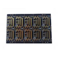
Mulitlayer Prited Wiring Board Thick Film Circuit Molded Circuit Board
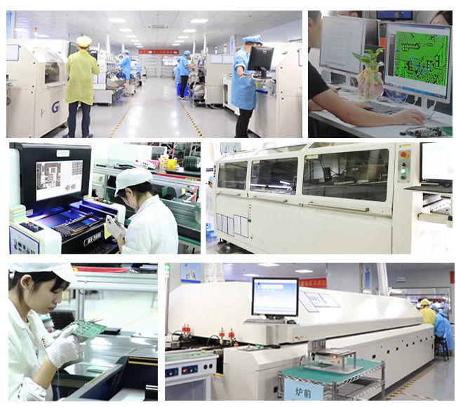
Shenzhen Yideyi Technology Co., Ltd is located in the beautiful scenery of Shenzhen city of Guangdong Province, it has modernized standard workshop of 9000 square meters, more than 500 employees, is a professional manufacturers of production of aluminum plate, single, double, multilayer printed circuit board and flexible circuit board.
We have a strong engineering team, high quality and efficient production and fast and global service in the industry are in a leading position, based on quality, service, efficiency and win-win, our processing products are widely used in computer, communication, auto parts products, medical equipment, precision instruments, aviation equipment, and other fields, we also provide the OEM service to customers in Europe and America, South Korea, Japan, Southeast Asia, the Middle East and Latin America. Companies adhering to thought of the “management of science and technology and creative enterprise”, continue develop new process and new products so that ahead of competition in the market. The perfect quality management system can provide a solid guarantee for us to produce high quality products. Our company can provide copy board, sample, mass production service, and provide the express production services for the customers and so on.
The multilayer PCB came into being due to the evolving changes in the electronics industry. The functions of electronics have become progressively more sophisticated over time, requiring more complex PCBs. Unfortunately, PCBs were limited by problems like noise, stray capacitance and crosstalk, and therefore needed to follow certain design constraints. These design considerations made it difficult to get a satisfactory level of performance from a single or even double-sided PCB - thus the multilayer PCB was born.
Packing the power of a double-layer PCB into a format that's a fraction of the size, multilayer PCBs are becoming increasingly popular in electronics. They come in a wide range of sizes and thicknesses to accommodate the needs of their expanding applications, with variants ranging anywhere from four to twelve layers. Layers most often come in even numbers, since odd numbers of layers can cause issues in the circuit like warping, and are no more cost-effective to produce. Most applications require between four and eight layers, though applications like mobile devices and smartphones tend to use around twelve layers, and some professional PCB manufacturers boast the ability to produce multilayer PCBs with nearly 100 layers. Multilayer PCBs with that many layers are rare to see, however, as they are extremely cost-inefficient.
While they do tend to be more expensive and labor-intensive to produce, multilayer PCBs are becoming an essential part of modern technology. This is primarily due to the host of benefits they offer, particularly in comparison to single and double-layer varieties.
Multilayer PCB Benefits
From a technical point of view, multilayer PCBs present several advantages in design. These benefits multilayer PCBs present include:
• Small Size: One of the most prominent and lauded benefits of using multilayer PCBs lies in their size. Because of their layered design, multilayer PCBs are inherently smaller than other PCBs with similar functionality. This presents a major benefit to modern electronics, as the current trend is working toward smaller, more compact yet more powerful gadgets like smartphones, laptops, tablets and wearables.
• Lightweight Construction: With smaller PCBs comes less weight, especially as the multiple connectors required to interlink separate single and double-layered PCBs are eliminated in favor of a multilayered design. This, again, is beneficial for modern electronics, which are geared more toward mobility.
• High-Quality: Due to the amount of work and planning that must go into the creation of multilayer PCBs, these types of PCBs tend to be better in quality than single and double-layer PCBs. They also
Our service
1. SMT service;
2. Design service, Gerber drawings;
3. Good quality and fast delivery with lower price than double side PCB.
4. Specifications of LEAD Free HASL 1 Layer / Single Side Rigid PCB/PCBA:
1) Base material: FR-1(94v0), FR-4, CEM-1,
2) Max Board size: 600*600mm
3) Board thickness: 0.2mm/0.6mm/0.8mm/1.2mm/1.6mm/3.2mm
4) Copper thickness: 0.5oz , 1oz , 2oz ,3oz,4oz, 5oz ,7oz , 11oz
5) Special tech: BGA, PTH, Blind and buried vias
6) Profile: V-scoring, V-cutting, punching, etching, milling, routing
7) Surface treatment: HASL, OS, Immersion gold, gold plated (coating)
8) With best price to USA, South American, India, South Africa and Europe
9) Main market: USA, EGYPT, Europe, South American, mid-east
10) Compliant: UL, ROHS, ISO9001-2000
11) Standard: IPC-A-600F, IPC-D-300G, MIL-STD-105D LEVEL II
12) Application: Home appliances, electronics, digital camera, LCD TV sets, medical equipments, telecommunication, LED lightings, street light, mobile phone, computer, laptop test equipment and power meter, electrical weighing scale, night
13) Small quantity and prototypes acceptable
14) Lead time: 5-7days for prototypes, 9-13days for mass production
15) Available Service: OEM, 24hrs service for fast prototype
SMT Production processes:
Material Receiving → IQC → Stock → Material to SMT → SMT Line Loading → Solder Paste/Glue Printing → Chip Mount → Reflow → 100% Visual Inspection → Automated Optical Inspection (AOI) → SMT QC Sampling → SMT Stock → Material to PTH → PTH Line Loading → Plated Through Hole → Wave Soldering → Touch Up → 100% Visual Inspection → PTH QC Sampling → In-Circuit Test (ICT) → Final Assembly → Functional Test (FCT) → Packing → OQC Sampling → Shipping
PCB Assembly Manufacturing Procedures:
Program Management
PCB Files → DCC → Program Organizing →Optimization → Checking
SMT Management
PCB Loader → Screen Printer → Checking → SMD Placement → Checking → Air Reflow → Vision Inspection → AOI → Keeping
PCBA Management
THT→Soldering Wave (Manual Welding) → Vision Inspection → ICT → Flash → FCT → Checking → Package → Shipment
Files Requested For Quote:
In order to provide you with the most efficient and accurate quote on manufacturing the requested unit, we ask that you provide us with the following information:
1. Gerber file,PCB file,Eagle file or CAD file are all acceptable
2. A detailed bill of materials (BOM)
3. Clear pictures of PCB or PCBA sample for us
4. Quantity and delivery required
5. Test method for PCBA to guarantee 100% good quality products.
6. Schematics file for PCB design if need to do function test.
7. A sample if available for better sourcing
8. CAD files for enclosure manufacturing if required
9. A complete wiring and assembly drawing showing any special assembly instructions if required
| Process | Item | Mass production capability | |
| SMT | Printing | Max PCB size | 900*600mm² |
| Max PCB weight | 8kg | ||
| Solder paste printing tolerance | ±25μm(6σ) | ||
| System repeat calibration tolerance | ±10μm(6σ) | ||
| Scraper pressure detection | pressure closed-loop control system | ||
| SPI | Detect Min BGA PAD to PAD distance | 100μm | |
| x-axis and Y-axis tolerance | 0.5μm | ||
| False Rate | ≤0.1% | ||
| Mount | Component size | 0.3*0.15 mm²--200*125 mm² | |
| Component max height | 25.4mm | ||
| BGA/CSP Min PAD spacing, and Min PAD diameter | 0.30mm,0.15mm | ||
| Populate tolerance | ±22μm(3σ),±0.05°(3σ) | ||
| PCB board size | 50*50 mm²-850*560 mm² | ||
| PCB thickness | 0.3mm--6mm | ||
| Populate Max components type | 500 | ||
| AOI | Detect Min components | 01005 | |
| Detect false type | Incorrect conponents,missing components,opposite direction,,component shift,Tombstone,Mounting on side,unsoldering,insufficient solder,Lead raised,Solder ball | ||
| Foot warping detection | 3D Detection function | ||
| Reflow | Temperature Accuracy | ±1ºC | |
| Welding protection | nitrogen protection;(remaining oxygen<3000ppm) | ||
| Nitrogen Control | Nitrogen closed-loop control system,±200ppm | ||
| 3D X-Ray | Magnification | Geometric Magnification;:2000 times;System Magnification:12000times | |
| Resolution | 1μm /nm | ||
| Rotation Angle &Slanting Perspective | Any ±45°+360°rotation | ||
| DIP | Preelaboration | Automatic forming technology | Component Automatic forming |
| DIP | DIP technology | Automatic Insertion machine | |
| Wave soldering | Wave soldering type | Ordinary wave soldering | |
| Inclination angle of transport guide rail | 4--7° | ||
| Temperature accuracy | ±3ºC | ||
| Soldering protection | nitrogen protection | ||
| Non-welding pressure contact technology | Max PCB board size | 800*600mm² | |
| Press down height accuracy | ±0.02mm | ||
| Pressure Range | 0-50KN | ||
| Pressure Accuracy | Standard value:±2% | ||
| Hold time | 0-9.999S | ||
| Conformal coating technology | Max PCB board size | 500*475*6mm | |
| Max PCB board weight | 5kg | ||
| Min Nozzle size | 2mm | ||
| Other characteristic | Conformal coating pressure Programmable control | ||
| ICT test | test level | Device level test,Test hardware connection status. | |
| Test point | >4096 | ||
| Test content | Contact test ,Open/short test,Resistance capacitance test test,diode, triode,mosfet test,No power on hybrid test,Boundary scan chain test,Power on mixed mode test. | ||
| Assembly and test | Production type | TWS | Mass production |
| Gaming controller | Mass production | ||
| Life Watch | Mass production | ||
| FT test | test level | PCB board system level test.Test System function status. | |
| Temperature cycling test | Temperature range | -60ºC--125ºC | |
| Rise/lower temperature rate | >10ºC/min | ||
| Temperature tolerance | ≤2ºC | ||
| Other Reliability test | burn-in test,Drop test, vibration test , Abrasion test ,Key life test. | ||

Trade Terms:
1. Payment: T/T in advance (Western Union , paypal is welcomed)
2. Production lead time 100PCS: 5-7days, 500~1000PCS: 7-10days, above 1000PCS 15-20days.
3. Sample can be delivered in 3days
4. Shipping freight are quoted under your requests
5. Shipping port: Shen zhen,Mainland China
6. Discounts are offered based on order quantities
7. MOQ: 1PCS
Package &Shipping Methods:
1. Vacuum package with silica gel, Carton box with packing belt.
2. By DHL, UPS, FedEx, TNT
3. By EMS
4. By sea for mass quantity according to customer's requirement
We are the smart choice for you and the trusted source at the center of your deal. Welcome the win-win situation together.

FAQ:
Q1. How to keep our product information and design file secret ?
We are willing to sign a NDA effect by customers side local law and
promising to keep customers data in high confidential level.
Q2. What file formats do you accept for production?
Gerber file: CAM350 RS274X
PCB file: Protel 99SE, P-CAD 2001 PCB
BOM: Excel (PDF,word,txt)
Q3. Please note that the following detail will speed up evaluation:
Material:
Board thickness:
Copper thickness:Surface finish:
Solder mask color:
Silkscreen color:
Q4. How to make sure the PCBAs are completely well recieved?
We will pack with aluminum bag, and insert card, up and bottom card
with stable cartons.
Q5. How to ship the PCBAs?
For small packages, we will ship the boards to you by
DHL,UPS,FEDEX,TNT. Door to door service! For mass production, we
could ship by air, by sea.
Q6. How to make sure the function is fine?
We could make sample/prototype and do functional testing before
mass production.


