
|
|
Trade Verify
Address: No.88 Shantong Road, Shanghai, China
Phone: 86-21-67291503-806
Contact name:Mr. Donny AN

Shanghai Rare Metal Advanced New Materials Co., Ltd |
|
Verified Suppliers
|
|
The New Horizon is Vertical in HB-LEDs.
Excimer Lasers Excel in Sapphire Substrate Removal.
Next generation vertical, GaN-based, highbrightness light emitting diodes (HB-LEDs) depend on sapphire growth substrate release. To this end, 248 nm excimer lasers provide second-to-none optical performance, and power and pulse stability ideal for fast, high yield laser lift-off (LLO) processing.
Introduction
The performance of commercial GaN-based, white-light HB-LEDs has
rocketed over the last decade (Fig.1) [1].
Relative cost and performance evolution of LEDs

Figure 1
Competition has fueled the creation of novel device
architectures with improved photon-extraction efficiencies, which
have increased the LED chip’s luminous flux, leading to
substantially reduced cost per lumen. This has opened up the range
of solid-state lighting applications for these devices,
and brought their characteristics in line with the
requirements for deployment in automotive, display
backlighting and general lighting.
Vertical Architectures
There are two fundamental ways to envisage an LED chip, i.e. a
lateral and a vertical die architecture (Fig.2). The choice of the
design is ultimately driven by the material.
Lateral and vertical LED designs

Figure 2
Sapphire is primarily used as the standard growth substrate
for the GaN layers due to its low cost and good lattice
matching. Sapphire is a good electrical insulator,
thus, the contacts are to be placed next to each other on the
front-side contacting the p- and the n-GaN layer, as depicted in
Fig.2 left. If, however, a conductive carrier material such as
copper, silicon or silicon carbide replaces the sapphire as carrier
substrate, a front-side and a back-side
contact is applicable resulting in a vertical design.
As a matter of fact, a vertical LED die (Fig.2, right),
involving removal of the non-conductive sapphire
substrate goes along with several inherent performance advantages
over the lateral LED approach [2]:
i) A vertical structure avoids the inhomogeneous current
distribution through the active multiple quantum well (MQW)
region including the current crowding towards the n-contact
as indicated in Fig.2 by the broad arrows.
ii) A vertical LED structure has a significant advantage in terms of substrate heat dissipation. This is key in obtaining higher light output from a single LED i.e. increasing the LED die size.
iii) In a vertical LED, the sapphire is lifted-off and does not
need to be diced. Moreover, with nondestructive excimer laser
lift-off removal of the sapphire wafer as a whole, the same
sapphire wafer can be used repetitively as GaN growth substrate.
This is a significant cost-saving aspect in HB-LED production.
A general aspect of HB-LEDs is the unavoidable
trapping of light inside the chip by total
internal reflection. Specific roughening of the emitting
surface of the vertical LED can reduce the internal reflection
losses by far. Such surface roughening is obtained e.g. in a wet
etching process following sapphire substrate removal carried out
using an excimer laser system.
Sapphire Substrate Removal via Laser Lift-Off
After epitaxial growth of the film stack and the patterning
of the LED chip, a carrier substrate of high thermal conductivity
is bonded to the p-layer side of the LED wafer (Fig.3).
This carrier wafer provides both good electrical contact and
good heat dissipation. Accordingly, silicon or a
specific metal alloy is employed. Substrate
transfer is completed by removing
the sapphire substrate via Laser Lift-Off (LLO). Since the
functional GaN layers are a few microns thin, chemical etching or
polishing of the sapphire wafer without damaging the GaN structure
is a cumbersome task with adverse effects on the overall yield.
Laser Lift-Off (LLO) is the method of choice for
obtaining selective separation that leaves the active
materials unaffected.
In the LLO process, the LED wafer is exposed to high intensity UV
laser light pulses directed through the sapphire
substrate, which is transparent at a wavelength of 248 nm
(Fig.3). GaN, however, strongly absorbs the UV photons in the
adjacent interface layer of ~20 nm in depth. At a laser fluence of
~600 mJ/cm2, the GaN interface layer locally heats up to ~1000°C
and decomposes into metallic gallium and nitrogen gas. Upon heating
the wafer to 30°C, Ga becomes liquid and the sapphire wafer can be
removed from the liquid interface [3].
Typical vertical LED manufacturing process flow

Figure 3
LLO with the Excimer Laser
The LLO process works by sequentially exposing areas of the wafer
to a single UV laser pulse until the entire surface area is
covered. The laser for LLO must meet requirements as to
wavelength, pulse energy and stability, in order to ensure a
controlled process.
i) First, it must emit pulsed UV-light with a
wavelength of below 350nm, since this corresponds to
the GaN bandgap of 3.5eV and is hence absorbed at the GaN
interface. UV laser technologies comprise excimer lasers at 248 nm,
and high harmonics of Nd:YAG lasers.
ii) Second, in order to enable a fluence of more than
600 mJ/cm2 over large per-shot-areas of several sq mm, high
laser pulse energies of 400 mJ or more are needed. The
per-shot-area is limited by the final size of the LED die which for
HB-LEDs can have an area of up to 5mm2. If the per shot-area is
larger or the LED dies are smaller in area, many dies can be
separated within a single laser shot (Fig.4).
Twelve LED dies separated with a single pulse (Photo: JPSA)

Figure 4
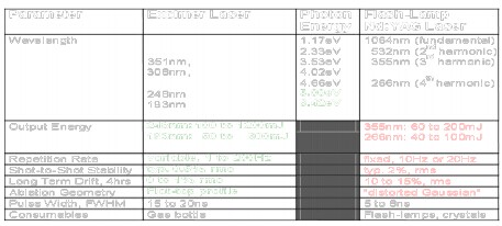
Excimer lasers directly emit UV laser pulses with high energy and
high peak power. They do not operate on higher harmonics like
Nd:YAG lasers. Thus, even compact excimer lasers put out more than
500 mJ/pulse whereas conversion efficiency
limits Nd:YAG pulses to 200 mJ even for powerful systems (Table 1).
Table 1: Excimer versus Nd:YAG laser parameters.
iii) A pivotal laser performance aspect in LLO processing is the
uniformity of the fluence over the entire per-short area.
Excimer lasers emit a large beam cross section and have inherently
low coherence. Their beam profile is shaped and homogenized by high
grade UV optics. The beam homogenizer is based on cylindrical
lenslets that homogenize the beam in
both axis individually. The combination of high quality
optics with the low coherence input beam of the excimer laser
results in a large, speckle-free field size with extremely
homogeneous fluence exhibiting a sharp fall-off at the edges
(Fig.5).
Excimer laser beam homogenization principle

Figure 5
The homogeneous field is subsequently demagnified by a factor of 5
and projected onto the wafer. System parameters of a 248 nm Laser
LiftOff system built on an LPXpro210 excimer laser and capable of
processing 50 wafers of 2” to 6” size per hour are summarized
below.
Table 2: Excimer laser lift-off system parameters

iv) Fluence uniformity is also to be maintained over consecutive
pulses setting severe pulse-to-pulse stability demand on the
laser.Whereas non-linear frequency conversion in Nd:YAG lasers
result in high pulse energy fluctuations of typically 2%,rms (Table
1), 248 nm excimer lasers deliver by far better pulse stability of
typically 0.5%,rms. Energy and power stability is maintained over
more than a hundred hours of non-stop excimer laser operation at
248 nm as shown in Figure 6.
Hands-free operation at 248nm over 120 hours.
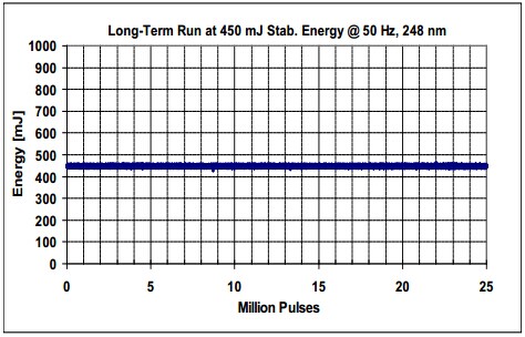
Figure 6
In advanced high power excimer lasers, virtually all
maintenance has been eliminated, except for automated gas
changing, which takes only a few minutes. Thus, maintenance costs
and downtime are comparable to state-of-the-art solid-state lasers
[4].
Conclusion and Outlook
HB-LEDs have started to compete with conventional light sources in
various markets. From a technical point of view, the general
lighting market requires a luminous efficacy beyond 100 lumens per
watt in a single die white LED package. Compared to lateral-type
LEDs, vertical-type LEDs have significant advantages, such as
better current injection, excellent heat dissipation, and
resistance to electrostatic discharge damage. Sapphire substrate
removal by excimer laser lift-off is an efficacy enhancing
technology which plays a vital role en route to manufacturing next
generation HBLEDs.
A trend in LED high volume manufacturing is the use of larger i.e.
6” wafers. Ultimately the LLO process must provide the throughput
to process six inch diameter wafers at a rate of 60 wafers
per hour. To this end, excimer laser technology at 248 nm is
available over a large output energy range up to 1 Joule/pulse. At
1 Joule pulse energy, about 400 pulses are necessary to
cover the entire 6” wafer in a lift-off process which is as fast as
10 seconds at 50 Hz pulse rate. Excimer laser lift-off
is thus an enabling technology, providing
throughput upscaling by larger illumination fields and higher
repetition rates.
References
[1] R. Haitz and J. Y. Tsao: Solid-state lighting: ‘The case’ 10
years after and future prospects; Phys. Status Solidi A 208, No. 1,
17–29 (2011).
[2] R.,Delmdahl, M. Kunzer, and U. Schwarz: Thin film LEDs gaining
ground. Excimer laser lift-off enables high brightness LED
production; Laser Technik Journal 3, 22- 25 (2011).
[3] C.-F. Chu et al.:Study of GaN light-emitting diodes fabricated
by laser lift-off technique; Journal of Applied Physics 95, No 8,
3916-3922 (2004).
[4] R. Delmdahl, R. Paetzel: The Midas Touch: Surface processing
with the UV excimer laser. Laser Technik Journal 1, 24-29 (2009)
This article belongs to "Coherent" and is for reference only, Shanghai Rare Metal do not take any responsibility on its authenticity.
Shanghai Rare Metal
Your strategic partner on high brightness LED chip metal substrate (CuW, CuMo, CuMoCu)