Active Member
|
[China]

Address: No.99 Tong Xi Road, Caijia Town, Beibei District, Chongqing,China
Contact name:Wu

Chongqing Silian Optoelectronic Science & Technology Co., Ltd. |
|
|
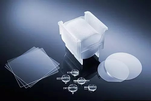
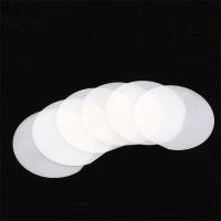
Different sizes of high-quality LED sapphire substrates
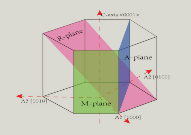
The composition of sapphire is alumina (A12O3), which is covalently bonded by three oxygen basals and two aluminum basals. The crystal structure is a hexagonal lattice structure. The optical penetration band of sapphire is very wide, from near ultraviolet light. (190nm) to mid-infrared rays have good light transmittance, and have the characteristics of high sound velocity, high temperature resistance, corrosion resistance, high hardness, high melting point (20452 degrees C), etc., and are often used as optoelectronic component materials. The quality of ultra-high-brightness white/blue LED depends on the material quality of gallium nitride epitaxy (GaN), so it is related to the surface processing quality of the sapphire substrate used. The lattice constant mismatch rate between the VI-deposited films is small, and it meets the high temperature resistance requirements of the GaN epitaxy process. Therefore, the sapphire substrate has become the key material for the production of white/blue/green LEDs.
| Wafer Surface Orientation | C-axis [0001] 0.35° |
| Mis-Orientation Towards Notch | -0.10° to 0.10° |
| Mis-Orientation Clockwise 90° from Notch | 0.35° ± 0.10° |
| Notch Orientation | M-plane (-1 1 0 0) |
| Diameter | 150.0mm ± 0.20mm |
| Thickness | 1.30mm ± 0.02mm |
| Notch Misalignment | -0.3° to 0.3° |
| GBIR | ≤ 15um |
| SBIR | ≤ 3um |
| Front Side Bow | -15 to 15um |
| Front Surface Finish | EPI Ready per INGN-0144 |
| Backsurface | Average Roughness: 0.65 to 0.95um Range of Roughness: 0.4um |
| Frontside Wafer ID | Wafer ID on front surface per SEMII T5-96 Text: MCXXXXXNNN-YZ MC: Silian 150mm wafer with 0.35 mis-orientation toward a-axis XXXXX: Clean Lot ID NNN: Wafer Number YZ: Checksum |
| Bevel Dimensions | Front Bevel Size: 50 to 150um Back Bevel Size: 50 to 200um Front Bevel Angle: 35 to 55 degree |
| ROA (at 0.5mm) | -1 to 1um |
| Surface Defects | PLLC 5183.0699 HC Candela Upper Spec Limits |
| Packaging: | Class 100 clean room environment, in cassettes of 25, under a nitrogen atmosphere. |
Product advantages
Pattern Sapphire Substrate (PSS): The sapphire substrate is designed to produce nano-scale specific regular microstructure patterns by growth or etching to control the output light form of the LED. At the same time, it can reduce the defects of the GaN grown on the sapphire substrate, improve the quality of the epitaxy, and improve the internal quantum efficiency of the LED and increase the light extraction efficiency.
It has the characteristics of high sound velocity, high temperature resistance, corrosion resistance, high hardness, high light transmittance, high melting point (2045°C), etc.