diameter 150mm 8inch 4inch 6inch Silicon-based AlN templates
500nm AlN film on silicon substrate
Applications of AlN template
Silicon-based semiconductor technology has reached its limits and
could not satisfy the requirements of future
electronic devices. As a typical kind of 3rd/4th-generation
semiconductor material, aluminum nitride (AlN) has
superior physical and chemical properties such as wide bandgap,
high thermal conductivity, high breakdown filed,
high electronic mobility and corrosion/radiation resistance, and is
a perfect substrate for optoelectronic devices,
radio frequency (RF) devices, high-power/high-frequency electronic
devices, etc.. Particularly, AlN substrate is the
best candidate for UV-LED, UV detectors, UV lasers, 5G
high-power/high-frequency RF devices and 5G SAW/BAW
devices, which could widely be used in environmental protection,
electronics, wireless communications, printing,
biology, healthcare, military and other fields, such as UV
purification/sterilization, UV curing, photocatalysis, coun
terfeit detection, high-density storage, medical phototherapy, drug
discovery, wireless and secure communication,
aerospace/deep-space detection and other fields.
we have developed a serials of proprietary processes and
technologies to fabricate
high-quality AlN templates. At present, Our OEM is the only
company worldwide who can produce 2-6 inch AlN
templates in large-scale industrial production capability with
capacity of 300,000 pieces in 2020 to meet explosive
market demand from UVC-LED, 5G wireless communication, UV detectors
and sensors etc
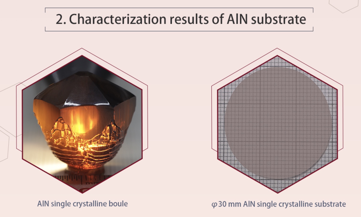
We currently provide customers with standardized
10x10mm/Φ10mm/Φ15mm/Φ20mm/Φ25.4mm/Φ30mm/Φ50.8mm high quality
nitrogen
Aluminum single crystal substrate products, and can also provide
customers with 10-20mm non-polar
M-plane aluminum nitride single crystal substrate, or customize
non-standard 5mm-50.8mm to customers
Polished aluminum nitride single crystal substrate. This product is
widely used as a high-end substrate material
Used in UVC-LED chips, UV detectors, UV lasers, and various high
power
/High temperature/high frequency electronic device field.
Specification
Characteristic Specification
- Model
UTI-AlN-030B-single crystal
- Diameter
Dia30±0.5mm ;
- Substrate thickness (µm)
400 ± 50
- Orientation
C-axis [0001] +/- 0.5°
Quality Grade
S-grade(super) P-grade(production)
R-grade(Research)
- Cracks
None
None
<3mm
- FWHM-2θXRD@(0002)
<150
<300
<500
- FWHM-HRXRD@(10-12)
<100
<200
<400
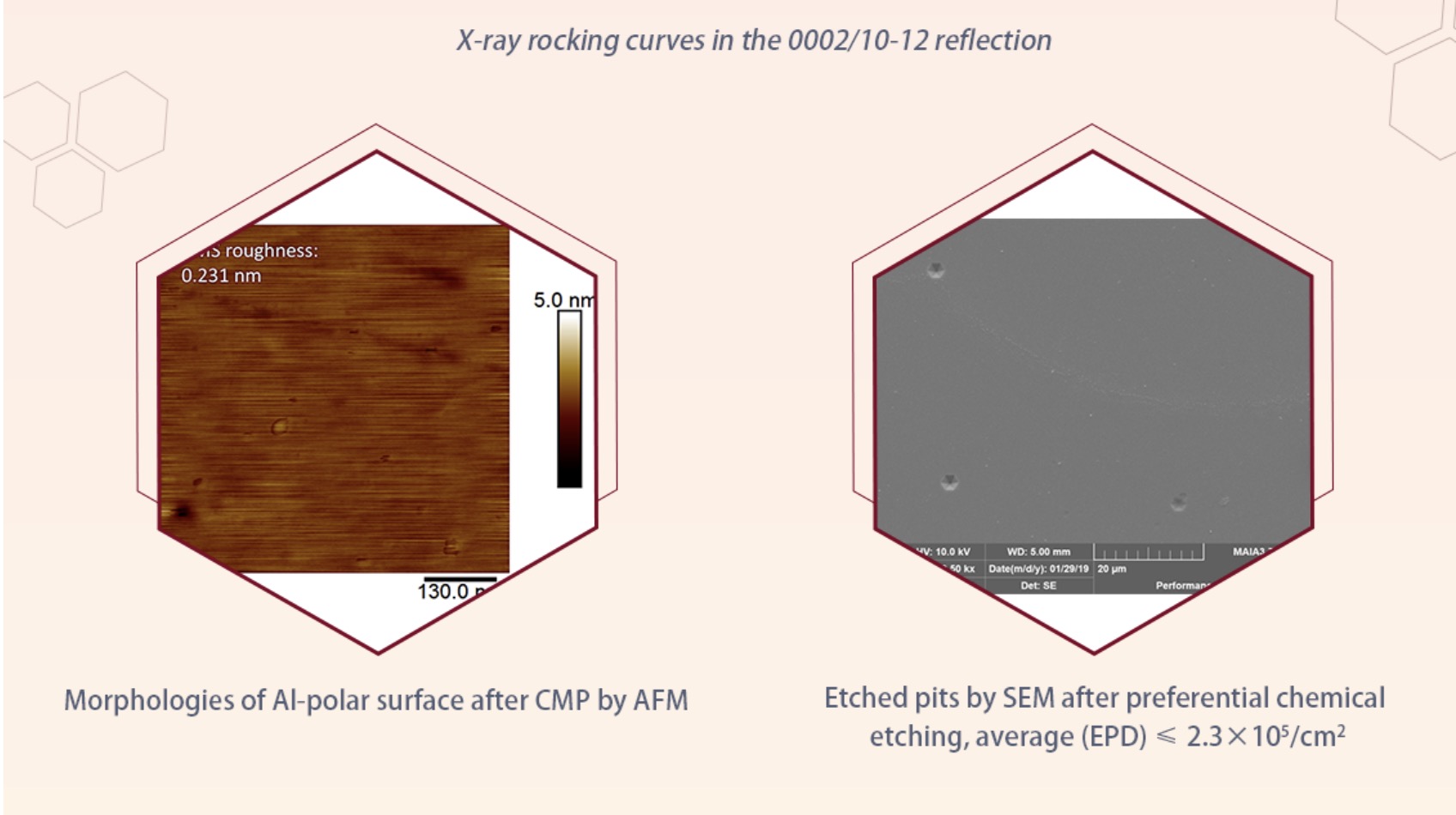
- Surface Roughness [5×5µm] (nm) Al-face <0.5nm; N-face(back surface)
<1.2um;
- Usable area
90%
- Absorbance
<50 ;
<70
;
<100;
- 1st OF length orientation
{10-10} ±5°;
- TTV (µm)
≤30
- Bow (µm)
≤30
- Warp (µm)
-30~30
- Note: These characterization results may vary slightly depending on
the equipments and/or software employed


impurity element C O Si B Na W P S Ti Fe
PPMW
27 90 5.4 0.92 0.23 <0.1 <0.1 <0.5 0.46 <0.5
| Crystal structure | Wurtzite |
| Lattice constant (Å) | a=3.112, c=4.982 |
| Conduction band type | Direct bandgap |
| Density (g/cm3) | 3.23 |
| Surface microhardness (Knoop test) | 800 |
| Melting point (℃) | 2750 (10-100 bar in N2) |
| Thermal conductivity (W/m·K) | 320 |
| Band gap energy (eV) | 6.28 |
| Electron mobility (V·s/cm2) | 1100 |
| Electric breakdown field (MV/cm) | 11.7 |