
|
|
[China]

Trade Verify
Address: Rm5-616,NO.851,Dianshanhu road; Qingpu area;shanghai city//201799
Contact name:Wang

SHANGHAI FAMOUS TRADE CO.,LTD |
|
Verified Suppliers
|
|
|
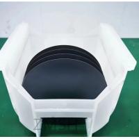
This product is a high-purity silicon wafer, designed specifically for the manufacture of high-performance integrated circuits. The wafer is processed through high-temperature melting and single-crystal growth, ensuring purity and crystal integrity. With strict surface treatment and quality control, the product demonstrates exceptional flatness and uniformity, providing a solid foundation for micro- and nano-processing. Its low impurity content and high electron mobility make it excel in high-frequency and high-speed electronic applications. This reliable and stable high-purity silicon wafer product has been recognized and applied by numerous semiconductor manufacturing enterprises worldwide.
Micro Motors: Employed as components in micro motors, applied in precision instruments and Micro-Electro-Mechanical Systems (MEMS).
Nanotechnology: high-purity silicon wafers used for the growth and processing of nanostructures.
Biotechnology: Serves as the base material for biosensors and microfluidic chips.
High-Frequency Microwave Components: high-purity silicon wafers used in the production of high-frequency microwave components for radar, communication, and navigation systems.
Semiconductor Lasers: Acts as the substrate material for semiconductor lasers.
Photo Detectors: high-purity silicon wafers used in the manufacture of photodetectors, applied in cameras, fiber-optic communications, etc.
Microwave Devices: Utilized in the production of various microwave devices, such as oscillators and amplifiers.
Fast Delivery: With efficient production and logistics, we ensure timely delivery of your order, helping you maintain project timelines.
Reliable Performance: Our high-purity silicon wafers are designed to deliver reliable and consistent performance, ensuring the success of your projects.
Innovative Solutions: We constantly innovate and improve our products, staying ahead of industry trends to provide you with cutting-edge solutions.
Sustainability: Committed to sustainability, our manufacturing processes are designed to minimize environmental impact.
Stringent Testing: Each high-purity silicon wafers undergoes stringent testing to ensure it meets our high standards of quality and performance.
Global Reach: With a global network, we are well-positioned to serve customers around the world, providing local support and expertise.
Trusted Reputation: With years of industry experience, we have built a reputation for quality, reliability, and customer satisfaction.
Extensive Research and Development: Our commitment to R&D ensures continuous improvement in our products, pushing the boundaries of what's possible.
Customer-Centric Approach: We prioritize our customers, tailoring our services and solutions to meet your unique needs and expectations.
These selling points highlight the quality, reliability, and innovation associated with high-purity silicon wafers, aiming to attract and reassure potential customers.
Parameter/Feature | Description/Specification |
Material Type | Single-Crystal Silicon |
Purity | 99.9999% (6N) or higher |
Diameter | 2 inch, 3 inch, 4 inch, 6 inch, 8 inch, 12 inch, etc. |
Thickness | Standard thickness or customized as per customer requirements |
Crystal Orientation | <100>, <111>, <110>, etc. |
Orientation Tolerance | ±0.5° or more precise |
Thickness Tolerance | ±5μm or more precise |
Flatness | ≤1μm or better |
Surface Roughness | <0.5nm RMS or lower |
Bending Strength | >500MPa |
Thermal Conductivity | <10/cm² or lower |
Coefficient of Thermal Expansion | ~2.6 × 10^-6 /°C |
Packaging | Vacuum packaging in a clean, dust-free environment |
Storage Conditions | Protected from light, in a dry environment, free of corrosive gases |
Applications | Semiconductor device manufacturing, optoelectronic devices, high-frequency equipment, micro/nano machining, etc. |

Silicon Carbide (SiC) Wafers are thin slices of semiconductor material primarily used for power electronics. To ensure the wafers are not damaged during shipping, it’s important to follow the proper packaging and shipping instructions.
Wafers must be shipped in an ESD safe package.
Each wafer should be wrapped in ESD safe material such as an ESD foam or bubble wrap.
The package should be sealed with ESD safe tape.
The package should be labeled with the ESD safe symbol and "Fragile" sticker.
The package should be shipped using a reliable courier service.
The package should be tracked to ensure it arrives at its destination safely.
The package should be labeled with the proper shipping address and contact information.


