
|
|
[China]

Trade Verify
Address: Rm5-616,NO.851,Dianshanhu road; Qingpu area;shanghai city//201799
Contact name:Wang

SHANGHAI FAMOUS TRADE CO.,LTD |
|
Verified Suppliers
|
|
|
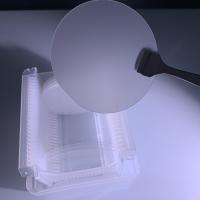
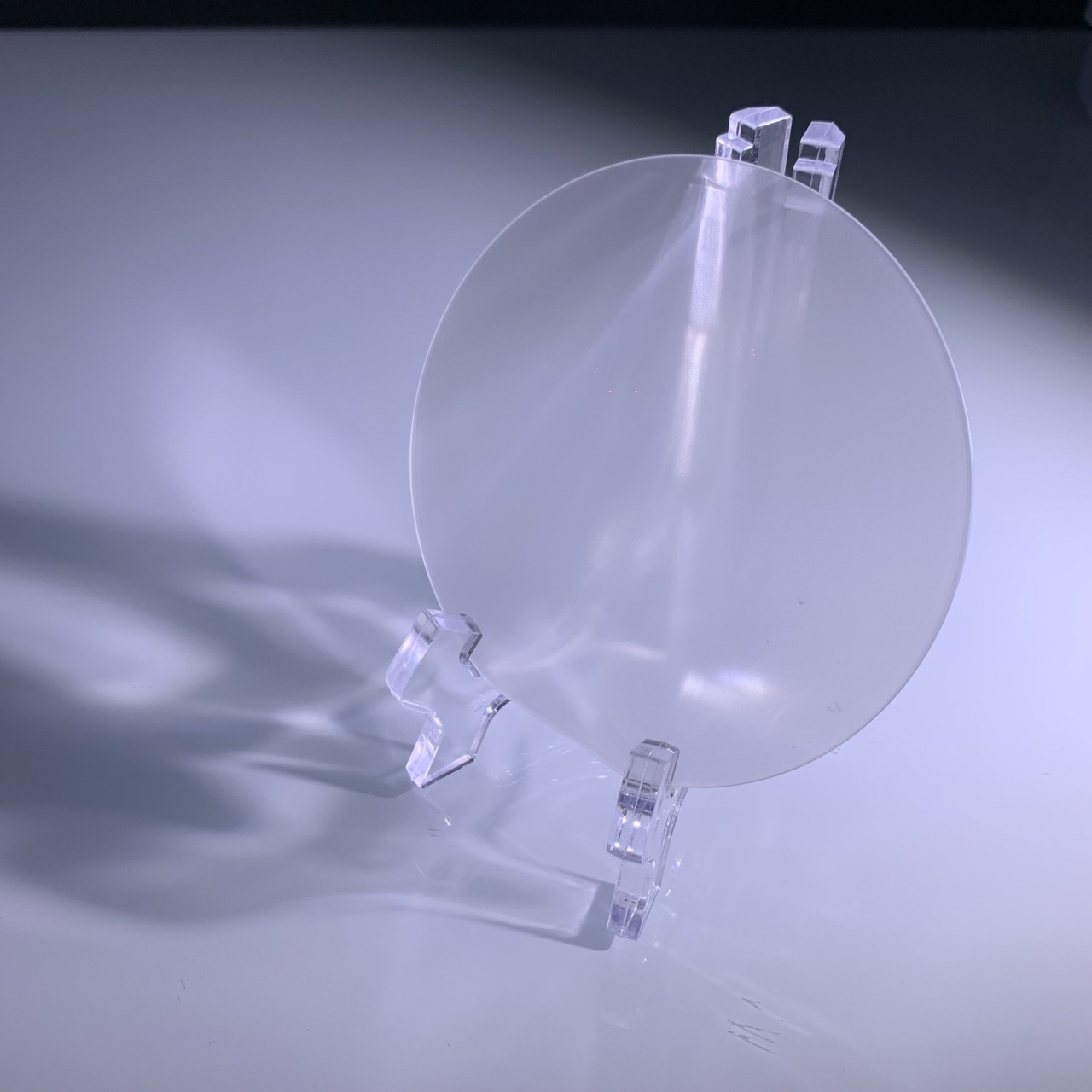
4inch 101.6mm Sapphire Wafer Substrate Carrier Single Side Polished Single Crystal Al2O3
4-inch sapphire wafer is widely used in LED, laser diode, optoelectronic devices, semiconductor devices, and other fields. The high light transmittance and high hardness of sapphire wafers make them ideal substrate materials for manufacturing high-brightness and high-power LEDs. In addition, sapphire wafers can also be used to manufacture optical Windows, mechanical components, and so on.
| Physical | |
| Chemical formula | Al2O3 |
| Density | 3.97 g/cm3 |
| Hardness | 9 Mohs |
| Melting point | 2050oC |
| Max. use temperature | 1800-1900oC |
| Mechanical | |
| Tensile strength | 250-400 MPa |
| Compressive strength | 2000 MPa |
| Poisson's ratio | 0.25-0.30 |
| Young's Modulus | 350-400 GPa |
| Bending strength | 450-860 MPa |
| Rapture Modulus | 350-690 MPa |
| Thermal | |
| Linear expansion rate (at 293-323 K) | 5.0*10-6K-1(⊥ C) |
| 6.6*10-6K-1(∥ C) | |
| Thermal conductivity (at 298 K) | 30.3 W/(m*K)(⊥ C) |
| 32.5 W/(m*K)(∥ C) | |
| Specific heat (at 298 K) | 0.10 cal*g-1 |
| Electrical | |
| Resistivity (at 298 K) | 5.0*1018 Ω*cm(⊥ C) |
| 1.3-2.9*1019 Ω*cm(∥ C) | |
| Dielectric constant (at 298 K, in 103-109 Hz interval) | 9.3 (⊥ C) |
| 11.5 (∥ C) | |
The production process for sapphire wafers usually includes the following steps:
Sapphire single crystal material with high purity is selected.
Cut sapphire single crystal material into crystals of appropriate size.
The crystal is processed into wafer shape by high temperature and pressure.
Precision grinding and polishing is performed many times to obtain high quality surface finish and flatness

| Specs | 2 inch | 4 inch | 6 inch | 8inch |
| Dia | 50.8 ± 0.1 mm | 100 ± 0.1 mm | 150 ± 0.1 mm | 200 ± 0.1 mm |
| Thick | 430 ± 25 um | 650 ± 25 um | 1300 ± 25 um | 1300 ± 25 um |
| Ra | Ra ≤ 0.3 nm | Ra ≤ 0.3nm | Ra ≤ 0.3nm | Ra ≤ 0.3 nm |
| TTV | ≤ 10um | ≤ 10um | ≤ 10um | ≤ 10um |
| Tolerance | ≤ 3 um | ≤ 3 um | ≤ 3 um | ≤ 3 um |
| Quality surface | 20/10 | 20/10 | 20/10 | 20/10 |
| Surface state | DSP SSP Grinding | |||
| Shape | Circle with notch or flatness | |||
| Chamfer | 45°,C Shape | |||
| Material | Al2O3 99.999% | |||
| N/O | Sapphire wafer | |||
The material is grown and orientated, and substrates are fabricated and polished to an extremely smooth damage free Epi-Ready surface on one or both sides of the wafer. A variety of wafer orientations and sizes up to 6" in diameter are available.
A-Plane sapphire substrates - are usually used for hybrid microelectronic applications requiring a uniform dielectric constant and highly insulating characteristics.
C-Plane substrates - tend to be used for all-V and ll-Vl compounds, such as GaN, for bright blue and green LED and laser diodes.
R-Plane substrates - these are preferred for the hetero-epitaxial deposition of silicon used in microelectronic IC applications.
Standard wafer 2 inch C-plane sapphire wafer SSP/DSP 3 inch C-plane sapphire wafer SSP/DSP 4 inch C-plane sapphire wafer SSP/DSP 6 inch C-plane sapphire wafer SSP/DSP | Special Cut A-plane (1120) sapphire wafer R-plane (1102) sapphire wafer M-plane (1010) sapphire wafer N-plane (1123) sapphire wafer C-axis with a 0.5°~ 4° offcut, toward A-axis or M-axis Other customized orientation |
Customized Size 10*10mm sapphire wafer 20*20mm sapphire wafer Ultra thin (100um) sapphire wafer 8 inch sapphire wafer | Patterned Sapphire Substrate (PSS) 2 inch C-plane PSS 4 inch C-plane PSS |
| 2inch | DSP C-AXIS 0.1mm/0.175mm/0.2mm/0.3mm/0.4mm /0.5mm/ 1.0mmt SSP C-axis 0.2/0.43mm (DSP&SSP) A-axis/M-axis/R-axis 0.43mm
|
| 3inch |
DSP/ SSP C-axis 0.43mm/0.5mm
|
| 4Inch |
dsp c-axis 0.4mm/ 0.5mm/1.0mm ssp c-axis 0.5mm/0.65mm/1.0mmt
|
| 6inch | ssp c-axis 1.0mm/1.3mmm
dsp c-axis 0.65mm/ 0.8mm/1.0mmt
|


Similar products:
In addition to 4-inch sapphire wafers, there are other sizes and shapes of sapphire wafers to choose from, such as 2-inch, 3-inch, 6-inch or even larger sapphire wafers. In addition, there are other materials that can be used to manufacture leds and semiconductor devices, such as aluminum nitride (AlN) and silicon carbide (SiC).


