
|
|
[China]

Trade Verify
Address: 6-11C Shidai Jingyuan,Fuyong, Baoan, Shenzhen, Guangdong, China 518103
Contact name:Ivy Deng

Bicheng Electronics Technology Co., Ltd |
|
Verified Suppliers
|
|
|
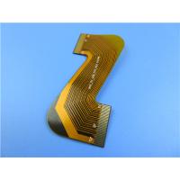
Flexible Printed Circuit (FPC) Built on 1oz Polyimide with Gold Plated and PI Stiffener for Modem USB
(Flexible printed circuits are custom-made products, the picture and parameters shown are just for reference)
General description
This is a type of 2 Layer flexible printed circuit (FPC) built on 1oz polyimide for the application of Modem USB.
Basic specifications
Base material: Polyimide 12.5μm + 0.2mm stiffener of polyimide
Layer count: 2 layers
Type: Individual FPC
Format: 55.0mm x 25.0mm = 1 type = 1 piece
Surface finish: Immersion gold
Copper weight: Outer layer 35μm/ Inner layer 0 μm
Solder mask / Legend: yellow coverlay / White
Final PCB height: 0.3 mm (inclusive of stiffener)
Standard: IPC 6012 Class 2
Packing: 100 pieces are packed for shipment.
Lead time: 10 working days
Shelf life: 6 months


Features and benefits
Weight reduction;
Consistency of assembly;
Reliability increased;
SMT process is resistant to reflow soldering, resistant to rework;
Powerful PCB capabilities support your research and development, sales and marketing;
30000 square meter month capability;
8000 types of PCB's per month;
Diversified shipping method: FedEx, DHL, TNT, EMS;
Applications
Mobile phone built-in antenna FPC, flexible flat cable, industrial control touch remote control soft board, display backlight, flex keyboard for mobile phone keys
General Properties of 2 Layer FCCL
| Test Item | Treatment Condition | Unit | Property Date | |||
| IPC Standard * value | Typical Value | |||||
| SF202 0512DT | SF202 1012DT | |||||
| Peel Strength (90º) | A | N/mm | ≥0.525 | 1.2 | 1.4 | |
| 288℃, 5s | ≥0.525 | 1.2 | 1.4 | |||
| Folding Endurance (MIT) | R0.8 X 4.9N | Times | - | >80 | >50 | |
| Thermal Stress | 288℃, 20s | - | - | No delamination | No delamination | |
| Dimensional Stability | MD | E-0.5/150 | % | ±0.2 | ±0.05 | ±0.05 |
| TD | ±0.05 | ±0.05 | ||||
| Chemical Resistance | After Chemical Exposure | % | ≥80 | >85 | >85 | |
| Dielectric Constant (1MHz) | C-24/23/50 | - | ≤4.0 | 3.2 | 3.3 | |
| Dissipation Factor (1MHz) | C-24/23/50 | - | ≤0.01 | 0.007 | 0.008 | |
| Volume Resistvitiy | C-96/35/90 | MΩ-cm | ≥10^6 | 4.5 x 10^8 | 3.5 x 10^8 | |
| Surface Resistance | C-96/35/90 | MΩ | ≥10^5 | 1.5 x 10^6 | 2.0 x 10^6 | |
Structure of FPC
According to the number of layers of conductive copper foil, FPC can be divided into single layer circuit, double layer circuit, multi-layer circuit, double sided and so on.
Single-layer structure: the flexible circuit of this structure is the simplest structure of the flexible PCB. Usually the base material (dielectric substrates) + transparent rubber(adhesive) + copper foil is a set of purchased raw materials(semi-manufactures), the protective film and transparent glue are another kind of bought raw material. First, copper foil must be etched to obtain the required circuit, and the protective film should be drilled to reveal the corresponding pad. After cleaning, the two are combined by rolling. Then the exposed part of the pad electroplated gold or tin to protect. In this way, the big panel board will be ready. Generally also it’s stamped into the corresponding shape of the small circuit board. There is also no protective film directly on the copper foil, but printed resistance soldering coating, so that the cost will be lower, but the mechanical strength of the circuit board will become worse. Unless the strength requirement is not high and the price needs to be as low as possible, it is best to apply the protective film method.
Double layer structure: when the circuit is too complex to be wired, or copper foil is needed to shield the ground, it is necessary to choose a double layer or even a multilayer. The most typical difference between a multilayer and a single plate is the addition of a perforated structure to connect the layers of copper foil. The first process of transparent rubber + base material + copper foil is to make holes. Drill holes in the base material and copper foil first, clean and then plated with a certain thickness of copper. The subsequent fabrication process is almost the same as the single-layer circuit.
Double sided structure: both sides of the double sided FPC have pads, mainly used to connect other circuit boards. Although it and monolayer structure is similar, but the manufacturing process is very different. Its raw material is copper foil, protective film and transparent glue. The protective film should be drilled according to the position of the pad first, then the copper foil should be affixed, the pad and track lines should be etched and then the protective film of another drilled hole should be affixed.


 Built on 1oz Polyimide with Gold Plated and PI Stiffener for Modem USB")
 Built on 1oz Polyimide with Gold Plated and PI Stiffener for Modem USB")
 Built on 1oz Polyimide with Gold Plated and PI Stiffener for Modem USB")
 Built on 1oz Polyimide with Gold Plated and PI Stiffener for Modem USB")
 Built on 1oz Polyimide with Gold Plated and PI Stiffener for Modem USB")
 Built on 1oz Polyimide with Gold Plated and PI Stiffener for Modem USB")