

Active Member
|
[China]

Address: Room 126-305, Building 2, Lixinhu Creative Park, No.1 Furui Road, Fuhai Subdistrict Bao'an District, Shenzhen, Guangdong, China
Contact name:Damon Liu

Shenzhen Betterliv Technology Co., Ltd. |
|
|
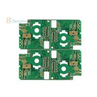
FR4 Double Side 6 Layer PCB Board Prototype Make Manufacturers OEM Multilayer PCB Boards
PCB Manufacture Capability
| Article | Description | Capability |
| Material | Laminate materials | FR4, High TG FR4, High Frequency, Alum, FPC... |
| Board Cutting | Number of layers | 1-48 |
| Min.thickness for inner layers (Cu thickness are excluded) | 0.003”(0.07mm) | |
| Board Thickness | Standard | (0.1-4mm±10%) |
| Min. | Single/Double:0.008±0.004” | |
| 4layer:0.01±0.008” | ||
| 8layer:0.01±0.008” | ||
| Bow and twist | no more than 7/1000 | |
| Copper Weight | Outer Cu weight | 0.5-4 0z |
| Inner Cu weight | 0.5-3 0z | |
| Drilling | Min size | 0.0078”(0.2mm) |
| Drill deviation | ±0.002″(0.05mm) | |
| PTH hole tolerance | ±0.002″(0.005mm) | |
| NPTH hole tolerance | ±0.002″(0.005mm) | |
| Solder Mask | Color | Green,white,black,red,blue… |
| Min solder mask clearanace | 0.003″(0.07mm) | |
| Thickness | (0.012*0.017mm) | |
| Silkscreen | Color | white,black,yellow,blue… |
| Min size | 0.006″(0.15mm) | |
| Max Size of Finish Board | 700*460mm | |
| Surface Finish | HASL,ENIG,immersion silver,immersion tin,OSP… | |
| PCB Outline | Square,circle,irregular(with jigs) | |
| Package | QFN,BGA,SSOP,PLCC,LGA | |
Our service
• Electronic components material purchasing
• Bare PCB fabrication
• PCB Assembly Service. (SMT, DIP)
• FULL Test: AOI, X-Ray, In-Circuit Test (ICT), Functional Test
(FCT)
• Conformal coating service
• Prototyping and mass production...
• PCB layout, PCBA design according to your idea
FAQ
Q1. What manufacturing services do you offer?
A1: We provide a one-stop full-turnkey manufacturing solution including PCB fabrication, component sourcing & procurement, SMT, plastic injection & metal, final assembly, testing, certification supports, and the other manufacturing services.
Q2. Could we sign the NDA before sending the files?
A2: Sure, we would like to sign the NDA (Non Disclosure Agreement) with our clients and keep the production files confidential.
Q3. What files do you need for the PCB & PCBA quotation?
A3: We need to know the Quantity inquiry, BOM, PCB Gerber, PCB specification requirement, pick and place file, Test plan (if you need). Then we will check and quote to you within 24hours, we would like to offer you the best price as we can.
Q4. What is the minimum order quantity for the PCBA order?
A4: Our PCBA MOQ is 1pcs, we could support you from the design sample verification to the mass production run. We are professional and willing to help you get all the manufacturing process fast and easily.


