
|
|
[China]

Trade Verify
Address: Room 1106, CIBC, No.198 Wuxing Rd, Hangzhou, P.R.China
Contact name:Xu

Hangzhou Freqcontrol Electronic Technology Ltd. |
|
Verified Suppliers
|

|
|
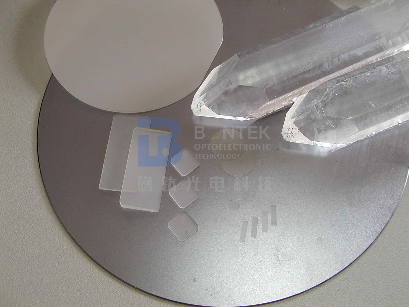
Single Crystal Quartz wafers/blanks are made of synthetic quartz crystal. It has good piezoelectric effect and is widely used in timing frequency control, frequency selection and QMEMS. Other applications include VCXO, TCXO, OCXO etc.
Material Characteristics
Material | Piezo / Optical grade |
Q-Value | Min 1.8x10^6, 2.4x10^6 to 3.0x10^6 IEC standards |
ECD | Max 2 /c㎡, 10/c㎡, Max 30/c㎡, Max 100/c㎡, Max 300/c㎡; Swept Quartz |
Inclusions Density | Ia, Ib, I, II, III Grades |
Swept | Both Pure Z and Y Bar available,with or without Swept quartz |
Processing capacity - blanks
| Cuts Type (orientation) | X, Y, Z, AT, BT, CT, ET ,DT, GT, NT, FC, SC, IT, AC, BC, ST, TS MT ,NT RT, LC…, etc |
| Angle Tolerance (±) | Theta Angle: ±5″, ±10″, ±15″, ±30″, ±1′, ±2′, …, etc. |
| Phi Angle: ±5′, ±10′, ±15′, ±30′, …, etc. | |
| Size | Round (3.0mm~8”)/ Square (1.6x1.6mm~48x48mm or larger)/ SMD (1.2x2.4mm Above) |
| Size Tolerance (±) | ±0.01mm,+/-0.005mm, +/-0.0005mm, according to size |
| Frequency/ Thickness | 1 Mhz up to 54Mhz for AT-Cut Fundamental; Up to 70Mhz by Etching |
| Flat | Per requested: the flat shall be perpendicular to X axis within ±10 deg |
| Surface Finishing | #1000(9u); #2000(7u); #3000(5u); #4000(3u) (Sic); Polished(Cerium oxide)& etched Std |
| Overtone | Fundamental; Third Overtone (3rd); Fifth Overtone (5th) |
| Contouring (dioptric) | Plano-Convex: 0.5 dioptric~10 dioptric Bi-Convex: 10 dioptric~15 dioptric |
Processing capacity - wafers
| Diameter | 3”(76.2mm) | 4”(100mm) | 6”(150mm) | 8”(200mm) |
| Thickness | 0.08mm Min-up | 0.10mm Min-up | 0.20mm Min -up | 0.35mm Min- |
| Primary Flat | 22mm | 32mm | 42.5mm | 57.5mm or notch |
| Surface | LTV (5mmx5mm) | <1.5µm | TTV | <1.5~3 µm |
| Bow | -30<bow<30 | Warp | <40µm | |
| Surface Type | SSP / DSP | Edge Criteria | R=0.2mm or Bullnose | |
| Polished side Ra | <0.5nm or per requested | Back Side Criteria | 0.2-0.5µm or as customized |


Acceptance Check

1. The product is fragile. We have adequately packed it and labeled it fragile. We deliver through excellent domestic and international express companies to ensure transportation quality.
2. After receiving the goods, please handle with care and check whether the outer carton is in good condition. Carefully open the outer carton and check whether the packing boxes are in alignment. Take a picture before you take them out.
3. Please open the vacuum package in a clean room when the products are to be applied.
4. If the products are found damaged during courier, please take a picture or record a video immediately. DO NOT take the damaged products out of the packaging box! Contact us immediately and we will solve the problem well.


