|
|
[China]

Trade Verify
Address: Room 1106, CIBC, No.198 Wuxing Rd, Hangzhou, P.R.China
Contact name:Xu

Hangzhou Freqcontrol Electronic Technology Ltd. |
|
Verified Suppliers
|

|
|
2 Inch C Plane 0001 430um Sapphire Single Crystal Wafers Polished Wafer
Sapphire is a single crystal of alumina and is the second-hardest material in nature, after diamond. Sapphire has good light transmittance, high strength, collision resistance, wear resistance, corrosion resistance and high temperature and high pressure resistance, biocompatibility, is an ideal substrate material for the production of semiconductor optoelectronic devices, the electrical properties of sapphire make it become the substrate material for the production of white and blue LED.
Our company's long-term production thickness ≧0.1mm, shape size ≧Φ2" high precision sapphire wafer. In addition to the conventional Φ2 ", Φ4 ", Φ6 ", Φ8 ", other sizes can be customized, please contact our sales staff.


| Item | 2-inch C-plane(0001) 430μm Sapphire Wafers | |
| Crystal Materials | 99,999%, High Purity, Monocrystalline Al2O3 | |
| Grade | Prime, Epi-Ready | |
| Surface Orientation | C-plane(0001) | |
| C-plane off-angle toward M-axis 0.2 +/- 0.1° | ||
| Diameter | 50.8 mm +/- 0.1 mm | |
| Thickness | 430 μm +/- 25 μm | |
| Primary Flat Orientation | A-plane(11-20) +/- 0.2° | |
| Primary Flat Length | 16.0 mm +/- 1.0 mm | |
| Single Side Polished | Front Surface | Epi-polished, Ra < 0.2 nm (by AFM) |
| (SSP) | Back Surface | Fine ground, Ra = 0.8 μm to 1.2 μm |
| Double Side Polished | Front Surface | Epi-polished, Ra < 0.2 nm (by AFM) |
| (DSP) | Back Surface | Epi-polished, Ra < 0.2 nm (by AFM) |
| TTV | < 10 μm | |
| BOW | < 10 μm | |
| WARP | < 10 μm | |
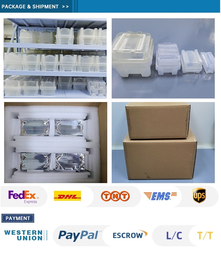
| Cleaning / Packaging | Class 100 cleanroom cleaning and vacuum packaging, | |
| 25 pieces in one cassette packaging or single piece packaging. | ||
| OPTICAL PROPERTIES of SAPPHIRE Al2O3 | |
Transmission Range | 0.17 to 5.5 microns |
Refractive Index | 1.75449 (o) 1.74663 (e) at 1.06 microns |
Reflection Loss | at 1.06 microns (2 surfaces) for o-ray - 11.7%; for e-ray - 14.2% |
Index of Absorption | 0.3 x 10⁻³ cm-1 at 2.4 microns |
dN/dT | 13.7 x 10⁻⁶ at 5.4 microns |
dn/dm = 0 | 1.5 microns |
| PHYSICAL PROPERTIES of SAPPHIRE Al2O3 | |
Density | 3.97 g/cm3 |
Melting Point | 2040 degrees C |
Thermal Conductivity | 27.21 W/(m x K) at 300 K |
Thermal Expansion | 5.6 x 10 -6 /K (parallel C-axis) & 5.0 (perpendicular C-axis) x 10 -6 /K |
Hardness | Knoop 2000 kg/mm 2 with 2000g indenter |
Specific Heat Capacity | 419 J/(kg x K) |
Dielectric Constant | 11.5 (parallel C-axis) 9.4 (perpendicular C-axis) at 1MHz |
Young's Modulus (E) | 335 GPa |
Shear Modulus (G) | 148.1 GPa |
Bulk Modulus (K) | 240 GPa |
Elastic Coefficients | C11=496 C12=164 C13=115 |
Apparent Elastic Limit | 275 MPa (40,000 psi) |
Poisson Ratio | 0.25 |
Orientation | R-plane, C-plane, A-plane, M-plane or a specified orientation |
Orientation Tolerance | ± 0.3° |
Diameter | 2 inches, 3 inches, 4 inches, 6 inches, 8 inches or others |
Diameter Tolerance | 0.1mm for 2 inches, 0.2mm for 3 inches, 0.3mm for 4 inches, 0.5mm for 6 inches |
Thickness | 0.25mm, 0.33mm, 0.43mm, 0.65mm, 1mm or others; |
Thickness Tolerance | 25μm |
Primary Flat Length | 16.0±1.0mm for 2 inches, 22.0±1.0mm for 3 inches, 30.0±1.5mm for 4 inches, 47.5/50.0±2.0mm for 6 inches |
Primary Flat Orientation | A-plane (1 1-2 0 ) ± 0.2°; C-plane (0 0-0 1 ) ± 0.2°, Projected C-Axis 45 +/- 2° |
TTV | ≤10µm for 2 inches, ≤15µm for 3 inches, ≤20µm for 4 inches, ≤25µm for 6 inches |
BOW | ≤10µm for 2 inches, ≤15µm for 3 inches, ≤20µm for 4 inches, ≤25µm for 6 inches |
Front Surface | Epi-Polished (Ra< 0.3nm for C-plane, 0.5nm for other orientations) |
Back Surface | Fine ground (Ra=0.6μm~1.4μm) or Epi-polished |
Packaging | Packaged in a class 100 clean room environment |