

Active Member
|
[China]

Address: Room 704-3, 7 / F, Building 9, Yard 8, Development Road, Changping District, Beijing
Contact name:Marina

Beijing Haina Lean Technology Co., Ltd |
|
|
Prototype printed circuit board (PCB) assemblies include surface-mount technology (SMT) PCB prototypes, PCBA prototype assembly, PCB sample assembly, etc. The term prototype PCB Assembly refers to a fast prototype PCBA used to test the function of new electronic designs.
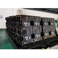
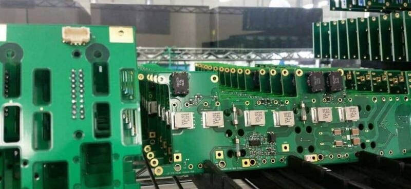
The prototype PCB assembly section of our manufacturing facility has a unique layout that allows for flexible use of both automated and manual parts-loading stations. Our engineers is qualified and experienced in producing surface-mount (SMT), through-hole (THT) and mixed-technology components and fine-pitch parts and ball grid arrays (BGAs) for high-density FR-4 PCBs .
Haina Lean Electronics Company is a professional manufacturer of printed circuit board. And is strong, trustworthy, abiding by contracts, guarantee our products' quality. The main products are PCB Layout, PCB design and PCBA (PCB'A) and enjoy a high position amony consumers. Ensure your timeliness, professional material proceurement team and fast warehouse. Haina Lean Electronics is your Trusted PCB Assembly Partner.
Our products are mainly exported to Europe and USA. Our customers spread over more than 80 countries. Products are widely used in various industries. many retailers and agents worldwide.
Assembly Types: Surface mount, Thro-hole, Mixed technology (SMT & Thru-hole), Single or double sided placement, Conformal coating, Shield cover assembly for EMI emission control
| FACTORY CAPABILITIES | |||
| No. | Items | 2019 | 2022 |
| 1 | HDI Capabilities | HDI ELIC (4+2+4) | HDI ELIC(5+2+5) |
| 2 | Max layer count | 32L | 36L |
| 3 | Board Thickness | Core thickness 0.05mm-1.5mm ,Fineshed board thickness 0.3-3.5mm | Core thickness 0.05mm-1.5mm ,Fineshed board thickness 0.3-3.5mm |
| 4 | Min.Hole Size | Laser 0.075mm Mechnical 0.15 | Laser 0.05mm Mechnical 0.15 |
| 5 | Min Line Width/Space | 0.035mm/0.035 | 0.030mm/0.030mm |
| 6 | Copper Thickness | 1/3oz-4oz | 1/3oz-6oz |
| 7 | Size Max Panel size | 700x610mm | 700x610mm |
| 8 | Registration Accuracy | +/-0.05mm | +/-0.05mm |
| 9 | Routing Accuracy | +/-0.075mm | +/-0.05mm |
| 10 | Min.BGA PAD | 0.15mm | 0.125mm |
| 11 | Max Aspect Ratio | 10:1 | 10:1 |
| 12 | Bow and Twist | 0.50% | 0.50% |
| 13 | Impedance Control Tolerance | +/-8% | +/-5% |
| 14 | Daily output | 3,000m2 (Max capacity of equipment) | 4,000m2 (Max capacity of equipment) |
| 15 | Surface Finishing | HASL Lead Free /ENEPING /ENIG /HASL /FINGER GOLD/IMMERSION TIN/SELECTIVE THICK GOLD | |
| 16 | Raw Material | FR-4/Normal Tg/High Tg/Low Dk/HF FR4/PTEE/PI | |
| PCBA Capability | |||
| Material Type | Item | Min | Max |
| PCB | Dimension (length,width,height.mm) | 50*40*0.38 | 600*400*4.2 |
| Material | FR-4,CEM-1,CEM-3,Aluminium-based board,Rogers,ceramic plate,FPC | ||
| Surface finish | HASL,OSP,Immersion gold,Flash Gold Finger | ||
| Components | Chip&IC | 1005 | 55mm |
| BGA Pitch | 0.3mm | - | |
| QFP Pitch | 0.3mm | - | |
Service value
Independent quotation system to quickly serve the market
PCB manufacturing
High-tech PCB and PCB assembly production line
Material purchasing
A team of experienced electronic component procurement engineers
SMT post soldering
Dust-free workshop, high-end SMT patch processing
Why choose us?
Welcome to visit our factory, Haina lean Electronics Co., Ltd.
1. Experienced: Focus on PCB And PCBA munufacturing over 10 years.
2. Professional: Expertise engineer with barrier-free English
3. Rapid delivery: On-time delivery rate reaches 98%
4.Cost effective: No excessive profits. Lower cost with same
quality And service

| Product Type | Qty | Normal lead time | Quick-turn lead time |
| SMT+DIP | 1-50 | 1WD-2WD | 8H |
| SMT+DIP | 51-200 | 2WD-3WD | 1.5WD |
| SMT+DIP | 201-2000 | 3WD-4WD | 2WD |
| SMT+DIP | ≥2001 | 4WD-5WD | 3WD |
| PCBA(2-4Layer) | 1-50 | 2.5WD-3.5WD | 1WD |
| PCBA(2-4Layer) | 51-2000 | 5WD-6WD | 2.5WD |
| PCBA(2-4Layer) | ≥2001 | ≥7WD | 5WD |
| PCBA(6-10Layer) | 1-50 | 3WD-4WD | 2.5WD |
| PCBA(6-10Layer) | 51-2000 | 7WD-8WD | 6WD |
| PCBA(10-HDILayer) | 1-50 | 7WD-9WD | 5WD |
| PCBA(10-HDILayer) | 51-2000 | 9WD-11WD | 7WD |
Our PCB SMT Assembly Military-Industrial Sphere ,Automotive /automobile , Medical .Communication Solution, Industrial Control, Aerospace , Image Processing ,video Processing Technology ,smart Home ,securit Etc.

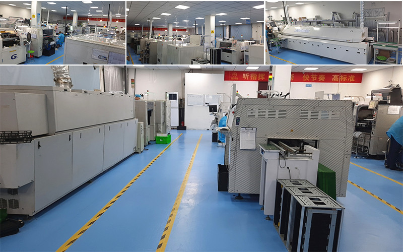
The company is equipped with advanced production lines, such as the
latest models from Japan’s YAMAHA, South Korea’s Samsung ,HELLER
,GKG-G5 ,AOI ,X-RAY,Online solder paste inspection/SPI machine
,Desen automatic screen printing machine and so on.
10 SMT high-speed production lines,
4 DIP production lines,
2 finished assembly lines.


PCB: Vacuum packaging with carton box
PCBA: ESD packaging with carton box


FAQ
Q1.What are needed for quotation?
PCB: Quantity, Gerber file and Technic
requirements(material,surface finish treatment, copper
thickness,board thickness ......)
PCBA: PCB information, BOM, (Testing documents...)
Q2. What file formats do you accept for production?
Gerber file: CAM350 RS274X
PCB file: Protel 99SE, P-CAD 2001 PCB
BOM: Excel (PDF,word,txt)
Q3.Are my files safe?
Your files are held in complete safety and security.We protect the
intellectual property for our customers in the whole process.. All
documents from customers are never shared with any third party.
Q4.MOQ?
There is no MOQ .We can flexibly handle small and mass production.
Q5.Shipping Cost ?
The shipping cost is determined by the destination ,weight ,packing size of the goods .We can provide shipping, air, land, express and other transportation services .
Q6.How to ensure high-quality production?
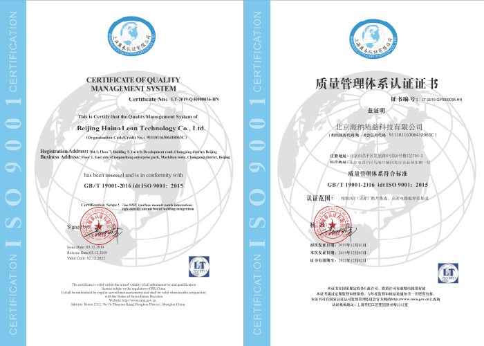
The process is strictly controlled under ISO 9001:2015 standards.
Most of our advanced equipment and tools are imported from abroad.
Such as Flying Probe, X-ray Inspection, AOI (Automated Optical
Inspector) and ICT (in-circuit testing).
We have a very professional QC team.
Q7.What are the services you can provide ?
One-stop contract manufacturing
A:PCB Assembly;
B:PCB Design & Layout
C:PCBA programming & functional testing;
D:Electronic components purchasing service;
E:Enclosure molding & final assembly with
labels,instructions,enclosure, boxes.
Q8.Whether all PCBA s will be tested before delivery ?
Yes , we will test each piece of PCBA product under your testing methods ,to ensure quality and functionality .
Q9.Do you provide OEM service ?
Yes ,we offer PCB and PCBA OEM/ODM Service , produce the PCB and PCBA products as your design and requirements .
Haina lean Electronics Co., Ltd is a one-stop EMS supplier integrating PCB design, PCB manufacturing, Component sourcing and PCB assembly.
Our company was established in May 1, 2012 in Beijing. And expansion was completed in June 2016. The company is specialized in electronic products supporting processing services, mainly to undertake circuit board design, layout production, components procurement, PCB plate making, circuit board welding assembly debugging and other OEM/ODM services.
Our first factory is located in Changping District, Beijing, the main radiation Haidian, Changping, Chaoyang three areas of Beijing. Since our company’s establishment, we have been adhering to creating high quality, high efficiency, low-cost business philosophy based on the circuit board processing industry for customers. Most of the key staff of the company are mature technical talents who have been engaged in the industry for more than 10 years, and have rich experience in the production of SMT and DIP, also has rich experience in production for high density & difficulty to package components such as BGA. The factory covers an area of 1500 square meters. Since its establishment, we obtain a good reputation in the industry through the continuous efforts of all staff and high quality service . Our second branch plant is located in Langfang city, and mainly cover Fengtai and Daxing Yizhuang area.
The company pursues "inclusiveness, excellence, people-oriented". Constantly innovate, take technology as the core, regard quality as life, and wholeheartedly provide customers with high-quality and high-efficiency humanized services.We are willing to serve our customers with the principle of continuous honesty & trustworthiness, pragmatism and innovation.
At present, the main cooperation industries are automotive electronics, communications, audio and video, optoelectronics, robotics, hydroelectric power, medical care, aerospace, education, radio frequency, power supply, printer etc industries.


