

Active Member
|
[China]

Address: Room 704-3, 7 / F, Building 9, Yard 8, Development Road, Changping District, Beijing
Contact name:Marina

Beijing Haina Lean Technology Co., Ltd |

|
|
4 Lay Pcb Protorype Quick Turn Printed Circuit Board Assembly Automotive PCBA
As a leading & professional quick turn pcb prototype factory in China, HAINA LEAN TECHNOLOGY CO., LTD provides one-stop pcba assembly service for customers, smart home PCBA, aerospace pcba, military PCBA, communication PCBA, industrial PCBA, automotive PCBA, medical PCBA etc. over 15 years.
With independent pcb factory in guangdong province and pcb assembly factory in beijing china, we can provide the most competitive pcb cost for middle and high-end customers. The whole pcb fabrication and assembly process is strictly comply with ISO & IATF certificates, safety,reliable and high yeild pcba obtained.
Specialized in assembling boards for Automotive Electronics, communication, Medical and industry control applications etc.
| FACTORY CAPABILITIES | |||
| No. | Items | 2019 | 2020 |
| 1 | HDI Capabilities | HDI ELIC (4+2+4) | HDI ELIC(5+2+5) |
| 2 | Max layer count | 32L | 36L |
| 3 | Board Thickness | Core thickness 0.05mm-1.5mm ,Fineshed board thickness 0.3-3.5mm | Core thickness 0.05mm-1.5mm ,Fineshed board thickness 0.3-3.5mm |
| 4 | Min.Hole Size | Laser 0.075mm | Laser 0.05mm |
| Mechnical 0.15mm | Mechnical 0.15mm | ||
| 5 | Min Line Width/Space | 0.035mm/0.035mm | 0.030mm/0.030mm |
| 6 | Copper Thickness | 1/3oz-4oz | 1/3oz-6oz |
| 7 | Size Max Panel size | 700x610mm | 700x610mm |
| 8 | Registration Accuracy | +/-0.05mm | +/-0.05mm |
| 9 | Routing Accuracy | +/-0.075mm | +/-0.05mm |
| 10 | Min.BGA PAD | 0.15mm | 0.125mm |
| 11 | Max Aspect Ratio | 10:1 | 10:1 |
| 12 | Bow and Twist | 0.50% | 0.50% |
| 13 | Impedance Control Tolerance | +/-8% | +/-5% |
| 14 | Daily Output | 3,000m2 (Max capacity of equipment) | 4,000m2 (Max capacity of equipment) |
| 15 | Surface Finishing | ENEPING /ENIG /HASL /FINGER GOLD/IMMERSION TIN/SELECTIVE THICK GOLD | |
| 16 | Raw Material | FR-4/Normal Tg/High Tg/Low Dk/HF FR4/PTEE/PI | |
| PCBA Capability | |||
| Material Type | Item | Min | Max |
| PCB | Dimension (length,width,height.mm) | 50*40*0.38 | 600*400*4.2 |
| Material | FR-4,CEM-1,CEM-3,Aluminium-based board,Rogers,ceramic plate,FPC | ||
| Surface finish | HASL,OSP,Immersion gold,Flash Gold Finger | ||
| Components | Chip&IC | 1005 | 55mm |
| BGA Pitch | 0.3mm | - | |
| QFP Pitch | 0.3mm | - | |
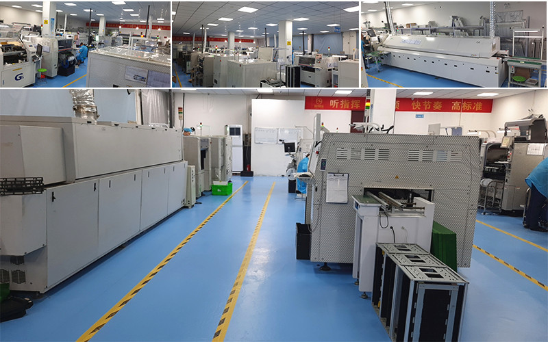
Our assembly process has been designed to meet all variations of PCBs, including single- or double-sided boards, Multilayer , rigid ,flexible circuits and Mixed technology. We run both leaded and RoHS/Lead-Free Surface Mount Technology (SMT) lines as well as wave solder equipment for both RoHS and leaded processes. Our manufacturing process allows for the highest quality product through process automation, environmental controls, automatic optical inspection (AOI) and flying probe at the best competitive price.

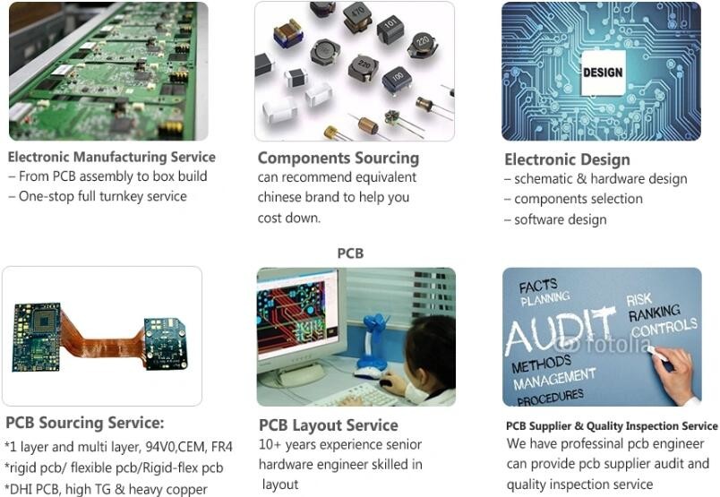
Electronic Manufacturing Service
PCB Electronic Design
PCB Layout Service
PCB Supplier & Quality Inspection Service
PCBA Components Sourcing
PCB Assembly process service
SMT and THT
Small/Medium/Large volume
Complex assemblies
AOI and X-Ray Inspection
Conformal coating
Turnkey or consigned or a mix as per customer’s requirments
PCBA Application Field
Used in automotive Printed circuit boards and PCB Assembly are
widey used in many other filed ,like communication industry,
power, security, optoelectronics, industrial control, medical
equipments and consumer electronics etc .


Haina lean Electronics provides custom test service according
to client's requirements and products.
Usually Haina lean Electronics Co.,Ltd PCBA Tech offers a full
range of testing service. Including:
1. AOI(Automatic Optical Inspection)
2. Function Testing
3. In Circuit Testing
4. Testing Jig
5. Testing Service
6. X-Ray for BGA Testing
7. Printing Solder Paste Test
Each board is carefully examined by our dedicated inspection team
using AOI and high magnification viewers.
Using our X-Ray machine, we test PCBs to component level and all
wiring is fully inspected and tested.
Flash testing and earth bonding tests can also be undertaken where
required.
Company Information
Beijing Haina lean Electronics Co.,Ltd is one of the most
professional PCB manufacturer in Beijing,China.
Our factory is providing high quality bare PCB, PCB layout design
service and PCB assembly service,including components sourcing,
function test,conformal coating and complete assembly for clients
all.
We have profuse experience in manufacturing PCB,owned experienced
technical R & D technology team, young and professional sales
and customer service team, experienced and professional procurement
team and assembly testing team, which make sure the products
quality of the pass rate, on-time delivery rate of customer orders.
Our services include: circuit board design and layout, 2-46 layers
PCB manufacturing, professional FPC production, electronic
components purchasing, SMT professional processing, Soldering and
Assembly, especially sample and small bulk orders. we have the
advantages of a quick quote, fast production, fast delivery.


