

Active Member
|
[China]

Address: Room 704-3, 7 / F, Building 9, Yard 8, Development Road, Changping District, Beijing
Contact name:Marina

Beijing Haina Lean Technology Co., Ltd |
|
|
Printed circuit board (PCB) assemblies include surface-mount technology (SMT) PCB prototypes, PCBA prototype assembly, PCB sample assembly, etc. The term prototype PCB Assembly refers to a fast prototype PCBA used to test the function of new electronic designs.
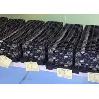
The prototype PCB assembly section of our manufacturing facility has a unique layout that allows for flexible use of both automated and manual parts-loading stations. Our engineers is qualified and experienced in producing surface-mount (SMT), through-hole (THT) and mixed-technology components and fine-pitch parts and ball grid arrays (BGAs) for high-density FR-4 PCBs .
Haina lean Electronics is a one-stop EMS supplier integrating PCB
design, PCB manufacturing, Component sourcing and PCB assembly.
The company is specialized in electronic products supporting
processing services, mainly to undertake circuit board design,
layout production, components procurement, PCB plate making,
circuit board welding assembly debugging and other OEM/ODM
services.
| FACTORY CAPABILITIES | |||
| No. | Items | 2019 | 2020 |
| 1 | HDI Capabilities | HDI ELIC (4+2+4) | HDI ELIC(5+2+5) |
| 2 | Max layer count | 32L | 36L |
| 3 | Board Thickness | Core thickness 0.05mm-1.5mm ,Fineshed board thickness 0.3-3.5mm | Core thickness 0.05mm-1.5mm ,Fineshed board thickness 0.3-3.5mm |
| 4 | Min.Hole Size | Laser 0.075mm Mechnical 0.15 | Laser 0.05mm Mechnical 0.15 |
| 5 | Min Line Width/Space | 0.035mm/0.035 | 0.030mm/0.030mm |
| 6 | Copper Thickness | 1/3oz-4oz | 1/3oz-6oz |
| 7 | Size Max Panel size | 700x610mm | 700x610mm |
| 8 | Registration Accuracy | +/-0.05mm | +/-0.05mm |
| 9 | Routing Accuracy | +/-0.075mm | +/-0.05mm |
| 10 | Min.BGA PAD | 0.15mm | 0.125mm |
| 11 | Max Aspect Ratio | 10:1 | 10:1 |
| 12 | Bow and Twist | 0.50% | 0.50% |
| 13 | Impedance Control Tolerance | +/-8% | +/-5% |
| 14 | Daily output | 3,000m2 (Max capacity of equipment) | 4,000m2 (Max capacity of equipment) |
| 15 | Surface Finishing | HASL Lead Free /ENEPING /ENIG /HASL /FINGER GOLD/IMMERSION TIN/SELECTIVE THICK GOLD | |
| 16 | Raw Material | FR-4/Normal Tg/High Tg/Low Dk/HF FR4/PTEE/PI | |
| PCBA Capability | |||
| Material Type | Item | Min | Max |
| PCB | Dimension (length,width,height.mm) | 50*40*0.38 | 600*400*4.2 |
| Material | FR-4,CEM-1,CEM-3,Aluminium-based board,Rogers,ceramic plate,FPC | ||
| Surface finish | HASL,OSP,Immersion gold,Flash Gold Finger | ||
| Components | Chip&IC | 1005 | 55mm |
| BGA Pitch | 0.3mm | - | |
| QFP Pitch | 0.3mm | - | |
PCB,Component sourcing ,QC ,SMT Process ,AOI ,Test ,Automatic optical inspection ,DIP Process ,Washing board ,FQC .


Printed circuit boards And PCB Assembly are mainly used for many telecom communication industry, medical equipments, consumer electronics ,automotive electronics, audio and video, optoelectronics, robotics, hydroelectric power, aerospace, education, power supply, printer ,Auto Industry ,Smart Home.etc.
| Product Type | Qty | Normal lead time | Quick-turn lead time |
| SMT+DIP | 1-50 | 1WD-2WD | 8H |
| SMT+DIP | 51-200 | 2WD-3WD | 1.5WD |
| SMT+DIP | 201-2000 | 3WD-4WD | 2WD |
| SMT+DIP | ≥2001 | 4WD-5WD | 3WD |
| PCBA(2-4Layer) | 1-50 | 2.5WD-3.5WD | 1WD |
| PCBA(2-4Layer) | 51-2000 | 5WD-6WD | 2.5WD |
| PCBA(2-4Layer) | ≥2001 | ≥7WD | 5WD |
| PCBA(6-10Layer) | 1-50 | 3WD-4WD | 2.5WD |
| PCBA(6-10Layer) | 51-2000 | 7WD-8WD | 6WD |
| PCBA(10-HDILayer) | 1-50 | 7WD-9WD | 5WD |
| PCBA(10-HDILayer) | 51-2000 | 9WD-11WD | 7WD |

PCB: Vacuum packaging with carton box
PCBA: ESD packaging with carton box

Q1:What service do you have?
A1: We provide turnkey solution including RD, PCB fabrication, SMT,
PCB Assembley ,final assembly,testing and other
value-added service.
Q2:What are the main products of your PCB/PCBA services?
A2:Our PCB/PCBA services are mainly for the industries including
Medical, Automotive, Energy,
Metering/Measurements. Consumer Electronics.
Q3:How can we ensure our information should not let third party to see our design?
A3: We are wiling to sign NDA effect by customer side locallaw and promising to keep customers datain highconfidential level.
Q4:What does Parason need for a customized PCB order?
A4:When you place a PCB order, the customers need to provide Gerber or pcb file.If you do not have the fileinthe correct format, you can send all the details related to the products.
Q5:What will be needed for a customized PCBA order?
A5: When you place a PCBA order, you need to provide Gerber or pcb file and the BOM list to us.
Q6:Do you have an minimum order quantity?
A6:We accept order with as low as a quantity of 1 (piece or panel)


