
|
|
[China]

Trade Verify
Address: RM1510, YUNHUA TIMES, Shajing Street, Baoan District, Shenzhen,Guangdong, China
Contact name:Yang

Huashengxin Circuit Limited |
|
Verified Suppliers
|
|
|
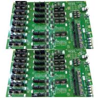
Printed Circuit Board Assembly Green Solder Mask PCB Assembly Automotive Green Energy Vehicle
PCBA Automotive PCB Board PCB Assembly
PCBA is the abbreviation of Printed Circuit Board + Assembly, which means that the empty PCB board passes through the SMT assembly, and then goes through the entire manufacturing process of the DIP plug-in, referred to as PCBA.
The PCBA process always starts out with the most basic unit of the PCB: the base, which consists of several layers, and each one plays a significant role in the functionality of the final PCB. These alternating layers include:
• Substrate: the base material of a PCB. It gives the PCB rigidity.
• Copper: A thin layer of conductive copper foil is added to each
functional side of the PCB — on one side if it's a single-sided
PCB, and on both sides if it's a double-sided PCB. This is the
layer of copper traces.
• Solder mask: On top of the copper layer is the solder mask, which
gives each PCB its characteristic green color. It insulates copper
traces from unintentionally contacting other conductive materials,
which could result in a short. The solder, in other words, keeps
everything in its place. Holes in the solder mask are where solder
is applied to attach components to the board. Solder mask is a
vital step for smooth manufacturing of PCBA since it stops
soldering from taking place on unwanted parts with shorts avoided.
• Silkscreen: A white silkscreen is the final layer on a PCB board.
This layer adds labels to the PCB in the form of characters and
symbols. It helps indicate the function of each component on
the board.
FAQ:
Q1:Are you a factory or trade company?
A: Yes, we are the factory, we have independent quick turn
prototype PCB manufacturing & big volume PCB production lines.
Q2:What kind of PCB file format can you accept for production?
A: Gerber, PROTEL 99SE, PROTEL DXP, POWER PCB, CAM350, ODB+(.TGZ)
Q3:Are my PCB files safe when I submit them to you for
manufacturing?
A: We respect customer's copyright and will never manufacture PCB
for someone else with your files unless we receive written
permission from your side, nor we'll share these files with any
other 3rd parties. And we could sign NDA with client if necessary.
Q4:If we have no PCB file/Gerber file, only have the PCB sample,can
you produce it for me?
A: Yes,we could help you to clone the PCB. Just send the sample PCB
to us, we could clone the PCB design and work out it.
Q5:What is your standard lead time for PCB?
A: Sample/prototype(less than 3sqm):
1-2 Layers: 3 to 5working days (fastest 24hours for quick turn
services)
4-8 Layers: 7~12 working days (fastest 48hours for quick turn
services)
Mass production (less than 200sqm):
1-2 Layers:7 to 12 working days
4-8 Layers:10 to 15 working days
Q6:What payment do you accept ?
A: Wire Transfer(T/T) or Letter of Credit(L/C) or Paypal(only for
small value less than 500usd)


