
|
|
[China]

Trade Verify
Address: Shenzhen YingSheng Technology Co., Ltd 805, Tongxin Technology Building, Qiaotou Community, Fuhai Street, Baoan District, Shenzhen
Contact name:Zhou

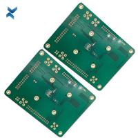
Shenzhen Yingsheng Technology Co., Ltd. |
|
Verified Suppliers
|
|
|
ine space/width of inner and outer circuit layers within 4mil (0.10mm), and PCB pad diameter within 0.35mm. For HDI PCBs, microvias can be single microvias, staggered vias, stacked vias, and skip vias, and because of microvias, HDI PCBs are also known as microvia PCBs. HDI PCB features blind microvias, fine traces, and sequential lamination manufacturing.
If you don't know the mentioned PCB vias for HDI PCBs, please refer to this post: 8 Types of PCB vias - A Complete Guide of PCB Vias in 2021.
HDI PCBs are usually classified by the HDI builds, and there are the 1+N+1, 2+N+2, 3+N+3, 4+N+4, and 5+N+5. In the HDI PCB's outer layers, microvias usually form the more expensive stacked vias or cheaper staggered vias.
Advantages of HDI PCB
The most common reason for using HDI technology is a significant
increase in packaging density.
The space obtained by finer track structures is available for components.
Besides, overall space requirements are reduced will result in smaller board sizes and fewer layers.
Usually FPGA or BGA are available with 1mm or less spacing.
HDI technology makes routing and connection easy, especially when routing between pins.
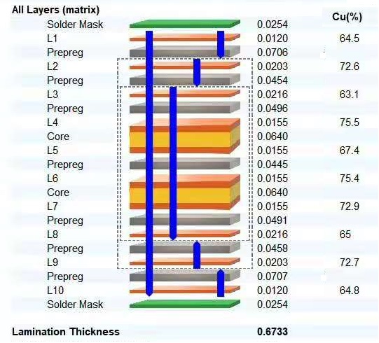
HDI PCB manufacturing methods vary depending on the HDI builds, and the common manufacturing is sequential laminating. The simplest 1+N+1 HDI PCB manufacturing is similar to multilayer PCB manufacturing. For example, a four-layer HDI PCB with a 1+2+1 structure is manufactured in this way:
1. The two inner PCB layers are manufactured and laminated, and the
two outer layers are manufactured.
2. The two inner layers are drilled by mechanical drilling. The two
outer layers are drilled by laser drilling.
3. Blind vias in the inner layers are electroplated. The two outer
layers are laminated with the inner layers.
For the 2+N+2 stacked via HDI PCBs, the common manufacturing method
is below (take a 2+4+2 HDI PCB as an example):
1. The 4 inner PCB layers are manufactured and laminated. Layer 2
and layer 7 are manufactured.
2. The inner layers are drilled by mechanical drilling. Layer 2 and
layer 7 are drilled by laser drilling.
3. Blind vias in the inner layers are electroplated. Layer 2 and
layer 7 are laminated with the inner layers.
4. Microvias in layer 2 and layer 7 are electroplated.
5. Layer 1 and layer 8 are manufactured. The HDI PCB manufacturer
locates the places for the microvias and drills by laser drilling.
6. Layer 1 and layer 8 are laminated with the finished PCB layers.
Manufacturing 2+N+2 staggered-via HDI PCBs is easier than 2+N+2
stacked-via HDI PCBs because the microvias do not require high
precision for locating and stacking.
In HDI PCB manufacturing, besides sequential laminating, technologies for creating stacked vias and in-hole metallization are also in use. For the higher HDI builds, the stacked vias in the outer layers can also be directly drilled by laser. But direct laser drilling requires extremely high precision for the drilling depth, and the scrap rate is high. So direct laser drilling is seldom applied.
| YScircuit HDI PCB manufacturing capabilities overview | |
| Feature | capabilities |
| Layer Count | 4-60L |
| Available HDI PCB Technology | 1+N+1 |
| 2+N+2 | |
| 3+N+3 | |
| 4+N+4 | |
| 5+N+5 | |
| Any layer | |
| Thickness | 0.3mm-6mm |
| Minimum line Width and Space | 0.05mm/0.05mm(2mil/2mil) |
| BGA PITCH | 0.35mm |
| Min laser Drilled Size | 0.075mm(3nil) |
| Min mechanical Drilled Size | 0.15mm(6mil) |
| Aspect Ratio for laser hole | 0.9:1 |
| Aspect Ratio for through hole | 16:1 |
| Surface Finish | HASL, Lead free HASL,ENIG,Immersion Tin, OSP, Immersion Silver, Gold Finger, Electroplating Hard Gold, Selective OSP,ENEPIG.etc. |
| Via Fill Option | The via is plated and filled with either conductive or non-conductive epoxy then capped and plated over |
| Copper filled, silver filled | |
| Laser via copper plated shut | |
| Registration | ±4mil |
| Solder Mask | Green, Red, Yellow, Blue, White, Black, Purple, Matte Black, Matte green.etc. |
| layer/m² | S<1㎡ | S<3㎡ | S<6㎡ | S<10㎡ | S<13㎡ | S<16㎡ | S<20㎡ | S<30㎡ | S<40㎡ | S<50㎡ | S<65㎡ | S<85㎡ | S<100㎡ |
| 1L | 4wds | 6wds | 7wds | 7wds | 9wds | 9wds | 10wds | 10wds | 10wds | 12wds | 14wds | 15wds | 16wds |
| 2L | 4wds | 6wds | 9wds | 9wds | 11wds | 12wds | 13wds | 13wds | 15wds | 15wds | 15wds | 15wds | 18wds |
| 4L | 6wds | 8wds | 12wds | 12wds | 14wds | 14wds | 14wds | 14wds | 15wds | 20wds | 25wds | 25wds | 28wds |
| 6L | 7wds | 9wds | 13wds | 13wds | 17wds | 18wds | 20wds | 22wds | 24wds | 25wds | 26wds | 28wds | 30wds |
| 8L | 9wds | 12wds | 15wds | 18wds | 20wds | 20wds | 22wds | 24wds | 26wds | 27wds | 28wds | 30wds | 30wds |
| 10L | 10wds | 13wds | 17wds | 18wds | 20wds | 20wds | 22wds | 24wds | 26wds | 27wds | 28wds | 30wds | 30wds |
| 12L | 10wds | 15wds | 17wds | 18wds | 20wds | 20wds | 22wds | 24wds | 26wds | 27wds | 28wds | 30wds | 30wds |
| 14L | 10wds | 16wds | 17wds | 18wds | 20wds | 20wds | 22wds | 24wds | 26wds | 27wds | 28wds | 30wds | 30wds |
| 16L | 10wds | 16wds | 17wds | 18wds | 20wds | 20wds | 22wds | 24wds | 26wds | 27wds | 28wds | 30wds | 30wds |


FQA
What is HDI PCBs?
High density interconnect (HDI) PCBs represent one of the fastest-growing segments of the printed circuit board market.
Because of its higher circuitry density, the HDI PCB design can incorporate finer lines and spaces, smaller vias and capture pads, and higher connection pad densities.
A high-density PCB features blind and buried vias and often contains microvias that are .006 in diameter or even less.
1.Multi-step HDI enables the connection between any layers;
2.Cross-layer laser processing can enhance the quality level of multi-step HDI;
3.The combination of HDI and high-frequency materials, metal-based laminates, FPC and other special laminates and processes enable the needs of high density and high frequency, high heat conducting, or 3D assembly.


