
|
|
[China]

Trade Verify
Address: Shenzhen YingSheng Technology Co., Ltd 805, Tongxin Technology Building, Qiaotou Community, Fuhai Street, Baoan District, Shenzhen
Contact name:Zhou

Shenzhen Yingsheng Technology Co., Ltd. |
|
Verified Suppliers
|
|
|
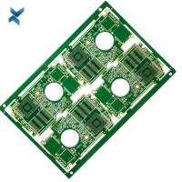
Advantages of HDI PCB
The most common reason for using HDI technology is a significant
increase in packaging density.
The space obtained by finer track structures is available for components.
Besides, overall space requirements are reduced will result in smaller board sizes and fewer layers.
Usually FPGA or BGA are available with 1mm or less spacing.
HDI technology makes routing and connection easy, especially when routing between pins.
| YScircuit HDI PCB manufacturing capabilities overview | |
| Feature | capabilities |
| Layer Count | 4-60L |
| Available HDI PCB Technology | 1+N+1 |
| 2+N+2 | |
| 3+N+3 | |
| 4+N+4 | |
| 5+N+5 | |
| Any layer | |
| Thickness | 0.3mm-6mm |
| Minimum line Width and Space | 0.05mm/0.05mm(2mil/2mil) |
| BGA PITCH | 0.35mm |
| Min laser Drilled Size | 0.075mm(3nil) |
| Min mechanical Drilled Size | 0.15mm(6mil) |
| Aspect Ratio for laser hole | 0.9:1 |
| Aspect Ratio for through hole | 16:1 |
| Surface Finish | HASL, Lead free HASL,ENIG,Immersion Tin, OSP, Immersion Silver, Gold Finger, Electroplating Hard Gold, Selective OSP,ENEPIG.etc. |
| Via Fill Option | The via is plated and filled with either conductive or non-conductive epoxy then capped and plated over |
| Copper filled, silver filled | |
| Laser via copper plated shut | |
| Registration | ±4mil |
| Solder Mask | Green, Red, Yellow, Blue, White, Black, Purple, Matte Black, Matte green.etc. |


FQA
What is HDI PCBs?
High density interconnect (HDI) PCBs represent one of the fastest-growing segments of the printed circuit board market.
Because of its higher circuitry density, the HDI PCB design can incorporate finer lines and spaces, smaller vias and capture pads, and higher connection pad densities.
A high-density PCB features blind and buried vias and often contains microvias that are .006 in diameter or even less.
1.Multi-step HDI enables the connection between any layers;
2.Cross-layer laser processing can enhance the quality level of multi-step HDI;
3.The combination of HDI and high-frequency materials, metal-based laminates, FPC and other special laminates and processes enable the needs of high density and high frequency, high heat conducting, or 3D assembly.


