
|
|
[China]

Trade Verify
Address: 3602, Unit 1, Building 2, Phase 3, Longhu Zichen Xiangsong, Huazhaobi Xiaheng Street, Jinniu District, Chengdu, China
Contact name:Sia Li

Chengdu Cesgate Technology Co., Ltd |
|
Verified Suppliers
|
|
|
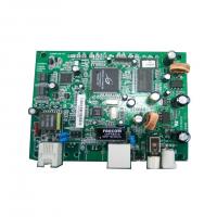
8 Layer Metalized Turnkey PCB Assembly ISO9001 Wifi Module Panel Circuit Board
PCB Surface Treatment
Since the copper surface of the turnkey PCB assembly is easily oxidized in the environment, it must be reprocessed and covered with a layer of coating on the exposed area that is not covered with solder mask ink to protect the process from oxidation. In response to various subsequent processing needs, various surface treatment processing methods with different materials, prices and different degrees of protection have been developed.
Common turnkey PCB assembly surface treatments include the following:
Bare copper plate, spray tin plate, lead-free spray tin plate, chemical gold plate, electroplating gold, chemical silver plate, OSP plate.

Technical Requirement for PCB Assembly:
1) Professional Surface-mounting and Through-hole soldering Technology
2) Various sizes like 1206, 0805, 0603 components SMT technology
3) ICT(In Circuit Test),FCT(Functional Circuit Test) technology.
4) Multilayer turnkey PCB assembly With CE, FCC, Rohs Approval
5) Nitrogen gas reflow soldering technology for SMT.
6) High Standard SMT&Solder Assembly Line
7) High density interconnected board placement technology capacity.
Specification
| Article | Description | Capability |
| Material | Laminate materials | FR4, High TG FR4, High Frequency, Alum, FPC... |
| Board Cutting | Number of layers | 1-48 |
| Min.thickness for inner layers (Cu thickness are excluded) | 0.003”(0.07mm) | |
| Board Thickness | Standard | (0.1-4mm±10%) |
| Min. | Single/Double:0.008±0.004” | |
| 4layer:0.01±0.008” | ||
| 8layer:0.01±0.008” | ||
| Bow and twist | no more than 7/1000 | |
| Copper Weight | Outer Cu weight | 0.5-4 0z |
| Inner Cu weight | 0.5-3 0z | |
| Drilling | Min size | 0.0078”(0.2mm) |
| Drill deviation | ±0.002″(0.05mm) | |
| PTH hole tolerance | ±0.002″(0.005mm) | |
| NPTH hole tolerance | ±0.002″(0.005mm) | |
| Solder Mask | Color | Green,white,black,red,blue… |
| Min solder mask clearanace | 0.003″(0.07mm) | |
| Thickness | (0.012*0.017mm) | |
| Silkscreen | Color | white,black,yellow,blue… |
| Min size | 0.006″(0.15mm) | |
| Max Size of Finish Board | 700*460mm | |
| Surface Finish | HASL,ENIG,immersion silver,immersion tin,OSP… | |
| PCB Outline | Square,circle,irregular(with jigs) | |
| Package | QFN,BGA,SSOP,PLCC,LGA | |
Who are we?
Small to medium volume PCB manufacturer
Multi PCB types manufacturer
EMS/PCBA/OEM customers reliable PCB partner
Trustworthy supplier for PCB trading companies
Powerful Factory, Quality First .
10 years PCB Manufacturer Experience .
Advanced Automation Production Facilities.
ISO9001, ISO14001 And UL Certified.


FAQ
| Q: Can we inspect quality during production? CESGATE: Yes, we are open and transparent on each production process with nothing to hide. We welcome customer inspect our production process and check in house. |
| Q: What does CESGATE need for a customized PCBA order? CESGATE: When you place a PCBA order, you need to provide Gerber or pcb file and the BOM list to us. |
| Q: Can your company provide the serial number when making circuit
board text? CESGATE: Serial numbers can be provided, and in addition to text serial numbers, QR-CODE can also be provided for customers to query. |
| Q: Which express companies do you cooperate with? CESGATE: We cooperate with express companies, including DHL, FedEX, UPS, TNT and EMS. And we also have our own freight forwarders, with lower shipping fees. |
| Q: What is the difference between the HDI board and the general
circuit board? CESGATE: Most of HDI use laser to form holes, while general circuit boards only use mechanical drilling, and HDI boards are manufactured by the build-up method (Build Up), so more layers will be added, while general circuit boards are only added once. |


