
|
|
[China]

Trade Verify
Address: 3602, Unit 1, Building 2, Phase 3, Longhu Zichen Xiangsong, Huazhaobi Xiaheng Street, Jinniu District, Chengdu, China
Contact name:Sia Li

Chengdu Cesgate Technology Co., Ltd |
|
Verified Suppliers
|
|
|
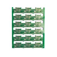
PCBA Circuit Board FR408 FR408HR FUJI NXT3 HDI PCB Min Trace 2.0mil Customized
In business since 2010, CESGATE mainly provides pcb fabrication and
design service for customers from all over the world. We have ISO
and UL certificate,and honored as HI-TECH enterprise by Chengdu
goverment.
As a professional PCB factory , we can provide prototype and
low-to-mid volume HDI PCB fabrication and design services for our
customers. We are in Chengdu, China, which is the largest center of
technology and electronics manufacturing in the world. Cooperating
with our engineering team, quality team, these allow us to offer
our customers low-cost, One-stop PCB Services.
Types and uses of HDI PCB
(A) 4-layer board
The substrate material is mainly epoxy glass fiber cloth. The main
uses are personal computers, medical electronic equipment,
measuring instruments, semiconductor testing machines, numerical
control machines, electronic switches, communication machines,
memory circuit boards, IC cards, etc.
(B) 6-8 layer board
The substrate material is still mainly epoxy resin glass fiber
cloth. Most of them are used in electronic switches, semiconductor
testing machines, mid-range personal computers, engineering
workstations and other machines.
(C) 10 layers or more
The material is mainly glass benzene resin material, or epoxy resin
is used as the multi-layer PCB substrate material. The application
of this type of PCB is special, and it is used in large industrial
computers, high-speed computers, defense machines, communication
machines, etc.
Why choose CESGATE?
QUALITY
All HDI PCB are 100% electrical tested. They can pick and send PCBs
to E-fixture test machines automatically, and place the PCBs at
appointed places after testing, according to the test result;All
PCBs are 100% visually inspected. All tests and inspect results are
recorded in the inspection report and shipped together with the
PCBs.
EXEPERIENCE
More than 10 years of experiences in the production of HDI PCB.
Professional Engineer and oversea sales team in the PCB industry
fully involved in the whole business procedures.Designed and
manufactured various complex PCBs, which can meet all your design
and manufacturing needs.
Equipment
More than 80% are automated production equipment, improves the
production efficiency and product quality.And a variety of famous
brand equipment is used in all processes, including Drilling,
Electroless Plating, Electroplating, Etching, Solder Mask, Silk
Screen, Chemical Gold, Electrolytic Gold, CNC Profiling,Electrical
Testing, and Packing.
Price
Since we are directly operated by the factory, intermediate links
are omitted. Secondly, we have a complete supply chain management
system to control the cost of production, manufacturing and
procurement sources. We will give you the cheapest purchase price
to compare with other factories or manufacturers while ensuring
good quality.
PCB Capacities and Technical Specification
| NO. | Items | Capabilities |
| 1 | Layers | 2-68L |
| 2 | Maximum machining size | 600mm*1200mm |
| 3 | Board thickness | 0.2mm-6.5mm |
| 4 | Copper thickness | 0.5oz-28oz |
| 5 | Min trace/space | 2.0mil/2.0mil |
| 6 | Minimum finished aperture | 0. 10mm |
| 7 | Maximum thickness to diameter ratio | 15:1 |
| 8 | Via treatment | Via, blind&buried via, via in pad, Copper in via … |
| 9 | Surface finish/treatment | HASL/HASL lead free, Chemical tin, Chemical Gold, Immersion gold Inmersion Silver/Gold, Osp, Gold Plating |
| 10 | Base Material | FR408 FR408HR, PCL-370HR;IT180A, Megtron 6(Panasonic);Rogers4350, Rogers4003, RO3003, Rogers/Taconic/Arlon/Nelco laminate with FR-4 material(including partial Ro4350B hybrid laminating with FR-4) |
| 11 | Solder mask color | Green.Black.Red.Yellow.White.Blue.Purple.Matte Green. Matte Black |
| 12 | Testing Service | AOI, X-Ray, Flying-Probe, Function Test, First Article Tester |
| 13 | Profiling Punching | Routing,V-CUT,Beveling |
| 14 | Bow&twist | ≤0.5% |
| 15 | HDI type | 1+n+1,2+n+2,3+n+3 |
| 16 | Min mechanical aperture | 0.1mm |
| 17 | Min laser aperture | 0.075mm |
Advanced PCB Manufacturing and PCB Assembly Equipment
CESGATE has imported the advanced machinery from US,Japan,German and Israel to improve our production and technical ability.We have set a great example the PCB field of flying probe testing,buried and blind via and special controlled impedance.We have a highly developed R&D division which has helped our factory successfully produce mechanical micro via,high density impedance and HDI.


FAQ
| Q: Why should we buy from CESGATE? CESGATE: Professional and experienced R&D team. Advanced production equipment, scientific and reasonable process flow. Reliable and strict quality control system. We test all our products before shipment to make sure everything is in perfect condition. From the design to the complete product, CESGATE's professional team will put you at ease |
| Q: IS PRODUCT PICTURES AND LABELS AVAILABLE? CESGATE: We will offer after you place an order or before shipment. |
| Q: WHAT IS YOUR TERMS OF PACKING? CESGATE: Generally, we pack our goods in neutral white boxes and brown cartons. |
| Q: WHAT IS YOUR MOQ? CESGATE: MOQ is SPQ normally, while it depends on your specific order. (Sample is available if the buyer can afford the shipping fee.) |
| Q: DO YOU TEST ALL YOUR GOODS BEFORE DELIVERY? CESGATE: 1. Our products are all original, and we will test the goods before shipment by professional machines like KEYSIGHT E4991A and KEYSIGHT E4980. 2. If The buyer need Test Report, we can send the product to anthoritative institution such as White horse Laboratories(SZ) Limited,Global Electronics Testing,etc. |


