

Active Member
|
[China]

Address: Building B, Shangxing West Industrial Zone, No. 1001, West Ring Road, Shajing street, Bao'an District, Shenzhen, Guangdong, China
Contact name:Yu

Quanhong FASTPCB |
|
|
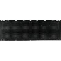
At present, LED display screens have been widely used in sports venues, squares, conferences and even streets and shopping malls. The NASDAQ full color screen in Times Square is the most famous. The screen covers an area of 120 feet ×90 feet, equivalent to 1005m, and is made of 19 million ultra-bright blue, green and red LEDS. In addition, in the securities market screen, bank exchange rate screen, interest rate screen and other aspects of the application also accounted for a large proportion, in the recent expressway, viaduct information screen also has a great development. The application of led in this field has become a large scale, forming a new industry, and can be expected to have a relatively stable growth.
| Item | HLC Advanced Technology | |||
| 2019 | 2020 | 2021 | ||
| Max Panel Width (inch) | 25 | 25 | 25 | |
| Max Panel Length (inch) | 29 | 29 | 29 | |
| Max Layer Count (L) | 16 | 18 | 36 | |
| Max Board thickness (mm) | 3.2 | 4 | 6 | |
| Max Board thickness Tolerance | +/-10% | +/-10% | +/-10% | |
| Base copper Thickness | Inner layer ( OZ ) | 4 | 6 | 8 |
| Outer Layer ( OZ ) | 2 | 3 | 4 | |
| Min DHS ( mm ) | 0.2 | 0.15 | 0.15 | |
| PTH Size Tolerance ( mil ) | +/-2 | +/-2 | +/-2 | |
| Back Drill (stub)( mil ) | ~ 3 | ~ 2.4 | ~ 2 | |
| Max. AR | 12:1 | 16:1 | 20:1 | |
| Item | HLC Advanced Technology | |||
| 2019 | 2020 | 2021 | ||
| M-drill tolerance | Inner layer ( mil ) | DHS + 10 | DHS + 10 | DHS + 8 |
| Outer Layer ( mil ) | DHS + 8 | DHS + 8 | DHS + 6 | |
| Solder mask Registration (um) | +/- 40 | +/- 30 | +/- 25 | |
| Impedance control | ≥50ohms | +/-10% | +/-10% | -/-8% |
| <50ohms | 5 Ω | 5 Ω | 4 Ω | |
| Min LW/S (Inner)@1oz base Cu ( mil ) | 3.0 / 3.0 | 2.6 / 2.6 | 2.5 / 2.5 | |
| Min LW/S (Outer)@1oz Cu ( mil ) | 3.5 / 3.5 | 3.0 / 3.5 | 3.0 / 3.0 | |
| Max dimple for POFV ( um ) | 30 | 20 | 15 | |
| Surface Finishing | ENIG, Immersion Ag, OSP, HASL, Immersion Tin, Hard Au | |||
| Item | HDI Advanced Technology | |||
| 2019 | 2020 | 2021 | ||
| Structure | 5+n+5 | 6+n+6 | 7+n+7 | |
| HDI Stack Via | AnyLayer(12L) | AnyLayer(14L) | AnyLayer(16L) | |
| Board Thickness(mm) | Min. 8L | 0.45 | 0.4 | 0.35 |
| Min. 10L | 0.55 | 0.45 | 0.4 | |
| Min. 12L | 0.65 | 0.6 | 0.55 | |
| MAX. | 2.4 | |||
| Min. Core Thickness ( um ) | 50 | 40 | 40 | |
| Min. PP Thickness ( um ) | 30(#1027PP) | 25(#1017PP) | 20(#1010PP) | |
| Base Copper Thickness | Inner Layer ( OZ) | 1/3 ~ 2 | 1/3 ~ 2 | 1/3 ~ 2 |
| Outer Layer ( OZ ) | 1/3 ~ 1 | 1/3 ~ 1 | 1/3 ~ 1 | |
| Item | HDI Advanced Technology | |||
| 2019 | 2020 | 2021 | ||
| Min. Mechanical Drill hole size(um) ** | 200 | 200 | 150 | |
| Max. Through Hole Aspect Ratio * | 8:1 | 10:1 | 10:1 | |
| Min. Laser via/Pad Size ( um ) | 75/200 | 70/170 | 60/150 | |
| Max. Laser Via Aspect Ratio | 0.8:1 | 0.8:1 | 0.8:1 | |
| Laser Via on PTH(VOP)design | Yes | Yes | Yes | |
| Laser X type through hole(DT≤200um) | NA | 60~100um | 60~100um | |
| Min. LW/S (L/S/Cu, um) | Inner Layer | 45 /45 /15 | 40/ 40/ 15 | 30/ 30 /15 |
| outer Layer | 50 /50/ 20 | 40 /50 /20 | 40 /40 /17 | |
| Min BGA Pitch (mm) | 0.35 | 0.3 | 0.3 | |
| Item | HDI Advanced Technology | |||
| 2019 | 2020 | 2021 | ||
| Solder mask Registration (um) | +/- 30 | +/- 25 | +/- 20 | |
| Min. Solder Mask Dam (mm) | 0.07 | 0.06 | 0.05 | |
| PCB Warpage Control | >= 50ohm | +/-10% | +/-8% | +/- 5% |
| < 50ohm | +/- 5ohm | +/- 3ohm | +/- 3ohm | |
| PCB Warpage Control | ≤0.5% | ≤0.5% | ≤0.5% | |
| cavity Depth accuracy (um) | Mechanical | +/- 75 | +/- 75 | +/- 50 |
| Laser directly | +/- 50 | +/- 50 | +/- 50 | |
| Surface Finishing | OSP,ENIG,Immersion Tin,Hard Au, Immersion Ag | OSP,ENIG,Immersion Tin,Hard Au,Immersion Ag, ENEPIG | ||
| Item | SMT Capability | |||
| 2019 | 2020 | 2021 | ||
| Min board thickness ( mm ) | 0.1 | 0.06 | 0.05 | |
| Max. board size ( mm ) | 200 x 250 | 250 x 300 | 250 x 350 | |
| Chip component ( L, C, R etc. ) | Minimum size | 1005 | 1005 | 1005 |
| Connector | 0.5 mm pitch | Y | Y | Y |
| 0.4 mm pitch | Y | Y | Y | |
| 0.35 mm pitch | Y | Y | Y | |
| High density component : | 0.5 mm pitch | Y | Y | Y |
| TSOP, QFP, QFN, LGA, BGA etc. | 0.4 mm pitch | Y | Y | Y |
| 0.35 mm pitch | Y | Y | Y | |
| Reflow | N2 reflow | No | Y | Y |
| Under-fill | Fill under chip | Manual | Auto | Auto |
| ACF attach | Gold finger pitch | N/A | 0.3 mm | 0.2 mm |
| Inspection | Component position, direction, missing etc. | Manual check with 10 x scope | Auto AOI inspection | Auto AOI inspection |
| Solder paste thickness | Measure once per shift | 1 line auto full area, online SPI | All lines auto full area, online SPI | |
| Packaging & Delivery | |||||
| Packaging Details: | Inner: vacuum packing or Anti-static package, Outer: export carton or according to the customer's requirement. | ||||
| Port: | Shenzhen or Hongkong | ||||
| Lead Time: | Quantity(Pieces) | 1-10 | 11-100 | 101-1000 | >1000 |
| Est. Time(days) | 3-5 | 3-5 | 7-9 | To be negotiated | |
FAQ:
Q: What service do you have?
FASTPCB: We provide turnkey solution including PCB fabrication,
SMT, plastic injection & metal,final assembly, testing and
other value-added service.
Q: What is needed for PCB & PCBA quotation?
FASTPCB: For PCB: Quantity, Gerber file and technic
requirements(material,size, surface finish treatment, copper
thickness,board thickness).
For PCB: PCB information, BOM,Testing documents.
Q: How to keep our product information and design file secret ?
FASTPCB: We are willing to sign a NDA effect by customers side
local law and promising tokeep customers data in high confidential
level.
Q: What are the main products of your PCB/PCBA services?
FASTPCB: Automotive, Medical, Industry Control, IOT, Smart Home,
Military, Aerospace.
Q: What is your minimum order quantity (MOQ)?
FASTPCB: Our MOQ is 1 PCS, sample and mass production all can
support.
Q: Are you factory?
FASTPCB:Shangxing West Industrial Zone, Xihuan Road, Shajing Street, Bao 'an District, Shenzhen, Guangdong province, China


