

Active Member
|
[China]

Address: A1-405 (Exit A, Fuyong Metro Station), Fuhai Information Port, Bao'an District, Shenzhen. 10mins from Shenzhen Bao'an International Airport by subway
Contact name:Cyan Hong

Shenzhen Lefang Electronics Co., Ltd |
|
|
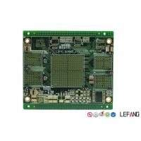
10 Layers PCB Prototype Quick Turn PCB OEM
The 2 mm board thickness 10 layers PCB Board is applied to consumer electronics. While the surface treatment of the PCB Board is ENIG with green solder mask. Also, the line width and spcaing of this PCB Circuit Board are both 0.1 mm, and the minimum aperture is 0.25 mm.
No.
| Item
| Data
|
| 1 | Layer count | 1-20 layers |
| 2 | Raw material type | Halogen free FR-4, high Tg FR-4, thick copper FR-4, CEM-3, copper
based, aluminum based |
| 3 | Raw material brand | Rogers,Isola,Arlon, ITEQ, Hitachi, SY, KB,etc |
| 4 | Board thickness | 0.1-6.0mm |
| 5 | Max board size | 600 mm * 700 mm |
| 6 | Solder mask | Green, red, blue, black, white, yellow |
| 7 | Surface treatment | HASL/HASL lead free , OSP, Immersion gold / silver / tin , gold plating
(hard gold and soft gold), silver plating, tin plating, platinum plating,
carbon ink, and ENEPIG(electroless nickel - electroless palladium -
immersion gold) |
| 8 | Copper thickness | 0.05 Oz - 8 Oz (17 um-288 um ) |
| 9 | Min Line width /space | 0.065 mm / 0.065 mm |
| 10 | Finished hole size | 0.10 - 5.95 mm |
| 11 | Blind/buried via | 0.10 mm |
| 12 | Aspect ratio | 10:1 |
| 13 | PTH tolerance | + / - 0.05 mm |
| 14 | Hole location tolerance | + / - 0.05 mm |
| 15 | Impedance control tolerance | + / - 8% mm |
| 16 | Outline tolerance | + / - 0.10 mm |
How to get quick quotation?![]()
| Step 1 Please send us Gerber file with these format: .CAD / .Gerber / .PCB / .DXP / .P-CAD, etc | ||||||||||||||||||||
| Step 2 Also please provide us the below details for quick quotation: | ||||||||||||||||||||
Board material: Fr - 4 / CEM - 1 / CEM - 3 / 22F / Fr - 1 / others | ||||||||||||||||||||
| Material brand: SY / KB / Rogers (optional) | ||||||||||||||||||||
| Material Specification:High Tg / copper based / aluminum based or others (optional) | ||||||||||||||||||||
| Board thickness: 0.1 - 6.0 mm | ||||||||||||||||||||
| Copper thickness: 0.05 Oz - 8 Oz ( 17 um - 288 um ) | ||||||||||||||||||||
| Surface Treatment: OSP / ENIG / HASL / Lead Free HASL / Immersion Tin / Immersion Sin | ||||||||||||||||||||
| Color of solder mask and silk print: Green / red / blue / black / white / yellow ,etc | ||||||||||||||||||||
| Board size and quantity | ||||||||||||||||||||
| ||||||||||||||||||||
SAMPLE: | ||||||||||||||||||||
| ||||||||||||||||||||
![]()
| AOI (Automated Optical Inspection) | Impedance control |
| Automatic short-circuit testing | Metallographic microscope |
| RoHS detector | Fly probe/ fixture mold |
| Dielectric tester | Visual inspection |
Now send us your inquiry, and you will be replied within 8 hours!
Size and quantity of the PCB hole
The PCB cost of the hold drilling is mainly depended on the hole diameter, drilling speed and error value. In the process of the PCB Board hole drilling, it will take a higher cost when the hole is smaller. And we suggest the hole size should be no less than 0.3mm.In addition, as for the aperture ratio, our suggestion is between 1/6 to 1/5. Because the PCB hole will be damage if the aperture ratio less than 1/8, which will increase the scrap rate. In the meanwhile, the more drilling hole in the PCBs, the higher cost will be taken place.


