

Active Member
|
[China]

Address: A1-405 (Exit A, Fuyong Metro Station), Fuhai Information Port, Bao'an District, Shenzhen. 10mins from Shenzhen Bao'an International Airport by subway
Contact name:Cyan Hong

Shenzhen Lefang Electronics Co., Ltd |
|
|
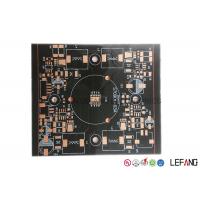
Single Layer / Double Layer Round Led Lights Circuit Custom LED Copper Base PCB
The copper base PCB are usually used in high heat generating application like LED lighting in the area of high power LED lighting, automotive interior, exterior lighting, parking garage lighting, LED spot light, etc. The specification of the copper base PCB board is 75 * 90 mm with black solder mask.
How to get quick quotation?
![]()
| Step 1 Please send us Gerber file with these format: .CAD / .Gerber / .PCB / .DXP / .P-CAD, etc | ||||||||||||||||||||
| Step 2 Also please provide us the below details for quick quotation: | ||||||||||||||||||||
Board material: Fr - 4 / CEM - 1 / CEM - 3 / 22F / Fr - 1 / others | ||||||||||||||||||||
| Material brand: SY / KB / Rogers (optional) | ||||||||||||||||||||
| Material Specification:High Tg / copper based / aluminum based or others (optional) | ||||||||||||||||||||
| Board thickness: 0.1 - 6.0 mm | ||||||||||||||||||||
| Copper thickness: 0.05 Oz - 8 Oz ( 17 um - 288 um ) | ||||||||||||||||||||
| Surface Treatment: OSP / ENIG / HASL / Lead Free HASL / Immersion Tin / Immersion Sin | ||||||||||||||||||||
| Color of solder mask and silk print: Green / red / blue / black / white / yellow ,etc | ||||||||||||||||||||
| Board size and quantity | ||||||||||||||||||||
If you don't have Gerber file, please provide us the imfomation as step 2 or post your PCB Board to us for clone.
| ||||||||||||||||||||
SAMPLE:
| ||||||||||||||||||||
| ||||||||||||||||||||
Technical Data
| Item | Details |
| Max layer count | 20 L |
| Max board thickness | 6.0 mm |
| Max aspect ratio | 10 : 1 |
| Max copper thickness | 6 OZ |
| Max dimension | 600 * 700mm |
| Min thickness of 4 layers PCB | 0.4 mm |
| Min hole / pad | 0.15 / 0.35mm |
| Hole location accuracy | + / - 0.05mm |
| PTH hole tolerance | + / - 0.05mm |
| Min line width and line space | 0.065 / 0.065mm |
| Surface treatment |
HASL / HASL lead free, OSP
Immersion gold/silver/tin, gold plating (hard gold and soft gold),
silver plating, tin plating, platinum plating, carbon ink,
ENEPIG (electroless nickel - electroless palladium - immersion gold) |
| Layer count | Sample lead time/workday | Batch lead time/workday |
| 1-2L | 2 | 6 |
| 4L | 5 | 8 |
| 6L | 5 | 9 |
| 8L | 6 | 10 |
| 10L | 8 | 10 |
| 12L | 8 | 12 |
| 14L | 10 | 15 |
| 16L | 10 | 18 |
| 18-40L (Up to difficulty) | at least 18 | at least 24 |
| P.S. For HDI, Blind/Buried Hole PCB: Regular Lead Time + 3 workdays | ||
How to guarantee our high quality products?
-- We employ 70 professional engineers to ensure our high quality products.
| Department | Headcount |
| Electronic Eng. | 13 |
| R&D Eng. | 15 |
| PE Eng. | 10 |
| CAM Eng. | 26 |
| MI Eng. | 6 |
Now send us your inquiry, and you will be replied within 8 hours!
Little knowledge - High Tg PCB
The glass transition temperature (Tg) is an important normative dimension for the base material that determines the temperature at which the resin matrix converts from a glassy, brittle condition into a soft, elastic one.
Normally high Tg refers to high heat resistance in PCB raw material.
The standard Tg for copper clad laminate is between 130 – 140℃. High Tg is generally greater than 170℃, and middle Tg is generally greater than 150℃. Basically the printed circuit board with Tg≥170℃, we call high Tg PCB.
The higher of TG value, the better of pcb high temperature resistance.


