

Active Member
|
[China]

Address: A1-405 (Exit A, Fuyong Metro Station), Fuhai Information Port, Bao'an District, Shenzhen. 10mins from Shenzhen Bao'an International Airport by subway
Contact name:Cyan Hong

Shenzhen Lefang Electronics Co., Ltd |
|
|
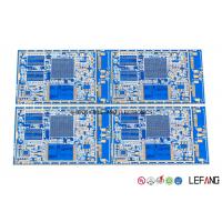
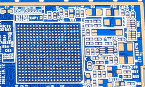
Car GPS Navigation Display Main board Automotive Fr4 PCB Circuit Board Blue Solder
Automotive increasingly relies on electronic components in the modern era. Most of the automotives are equipped with GPS system. LEFANG is experienced in automotive GSP PCB manufacturing, certificated as ISO / TS 16949. For the 8 layers Automotive PCB Circuit Board, it is a GPS Navigation Display Main board with immersion gold surface treatment and blue solder mask.
Established in 1999, Lefang owns 3 modern Printed Circuit Board factories in Guangdong, China.
We provide One-stop solution for PCB & PCBA manufacturing to our customers home and abroad.
High quality PCB products, competitive price, on time delivery, after-sale service are always offered.
To make the continued progress, we try our best to in every section, including selecting quality raw materials
strictly, imported advanced automated equipments, employing 70 experienced engineers, acquiring global
certification of ISO9001:2008, ISO14001:2004, ISO/TS16949:2009, UL, QC080000, OHSA18000, etc.
Our customers' industry come from Communication, Industrial Control, Automotive, Medical Equipment,
Security Apparatus, Consumer Electronics and LED Lighting.
We sincerely pursue win-win business with customer all the time!
![]()
| Step 1 Please send us Gerber file with these format: .CAD / .Gerber / .PCB / .DXP / .P-CAD, etc | ||||||||||||||||||||
| Step 2 Also please provide us the below details for quick quotation: | ||||||||||||||||||||
Board material: Fr - 4 / CEM - 1 / CEM - 3 / 22F / Fr - 1 / others | ||||||||||||||||||||
| Material brand: SY / KB / Rogers (optional) | ||||||||||||||||||||
| Material Specification:High Tg / copper based / aluminum based or others (optional) | ||||||||||||||||||||
| Board thickness: 0.1 - 6.0 mm | ||||||||||||||||||||
| Copper thickness: 0.05 Oz - 8 Oz ( 17 um - 288 um ) | ||||||||||||||||||||
| Surface Treatment: OSP / ENIG / HASL / Lead Free HASL / Immersion Tin / Immersion Sin | ||||||||||||||||||||
| Color of solder mask and silk print: Green / red / blue / black / white / yellow ,etc | ||||||||||||||||||||
| Board size and quantity | ||||||||||||||||||||
If you don't have Gerber file, please provide us the imfomation as step 2 or post your PCB Board to us for clone.
| ||||||||||||||||||||
SAMPLE:
| ||||||||||||||||||||
| ||||||||||||||||||||
Lead Time
| Layer count | Sample lead time/workday | Batch lead time/workday |
| 1-2L | 2 | 6 |
| 4L | 5 | 8 |
| 6L | 5 | 9 |
| 8L | 6 | 10 |
| 10L | 8 | 10 |
| 12L | 8 | 12 |
| 14L | 10 | 15 |
| 16L | 10 | 18 |
| 18-40L (Up to difficulty) | at least 18 | at least 24 |
| P.S. For HDI, Blind/Buried Hole PCB: Regular Lead Time + 3 workdays | ||
-- We employ 70 professional engineers to ensure our high quality products.
| Department | Headcount |
| Electronic Eng. | 13 |
| R&D Eng. | 15 |
| PE Eng. | 10 |
| CAM Eng. | 26 |
| MI Eng. | 6 |
Now send us your inquiry, and you will be replied within 8 hours!
Little knowledge - Multilayer PCB Board
Multilayer printed circuit boards (Multilayer PCBs) represented the next major evolution in fabrication technology.
A very sophisticated and complex methodology came from the base platform of double sided plated.
This methodology would again allow circuit board designers a dynamic range of interconnects and applications.
Multilayer PCB board were essential in the advancement of modern computing, and their basic construction and fabrication are similar to micro chip fabrication on a micro size.
The range of material combinations is extensive from basic epoxy glass to exotic ceramic fills, and it can be built on ceramic, copper, and aluminum. Also, blind and buried vias are commonly produced in multilayer pcb manufacturing, along with pad on via technology.


