

Active Member
|
[China]

Address: A1-405 (Exit A, Fuyong Metro Station), Fuhai Information Port, Bao'an District, Shenzhen. 10mins from Shenzhen Bao'an International Airport by subway
Contact name:Cyan Hong

Shenzhen Lefang Electronics Co., Ltd |
|
|
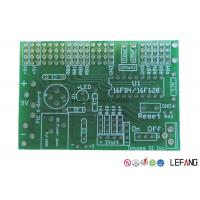
Double Sided Lead Free HASL 2 OZ Heavy Copper PCB Circuit Board with Green Ink
The green ink heavy copper PCB is a double sided 2 layers printed circuit board with 1.6 mm board thickness. While its copper thickness iS 2 OZ/ 70 µm, which allows a higher current to go through.
![]()
| Step 1 Please send us Gerber file with these format: .CAD / .Gerber / .PCB / .DXP / .P-CAD, etc | ||||||||||||||||||||
| Step 2 Also please provide us the below details for quick quotation: | ||||||||||||||||||||
Board material: Fr - 4 / CEM - 1 / CEM - 3 / 22F / Fr - 1 / others | ||||||||||||||||||||
| Material brand: SY / KB / Rogers (optional) | ||||||||||||||||||||
| Material Specification:High Tg / copper based / aluminum based or others (optional) | ||||||||||||||||||||
| Board thickness: 0.1 - 6.0 mm | ||||||||||||||||||||
| Copper thickness: 0.05 Oz - 8 Oz ( 17 um - 288 um ) | ||||||||||||||||||||
| Surface Treatment: OSP / ENIG / HASL / Lead Free HASL / Immersion Tin / Immersion Sin | ||||||||||||||||||||
| Color of solder mask and silk print: Green / red / blue / black / white / yellow ,etc | ||||||||||||||||||||
| Board size and quantity | ||||||||||||||||||||
If you don't have Gerber file, please provide us the imfomation as step 2 or post your PCB Board to us for clone.
| ||||||||||||||||||||
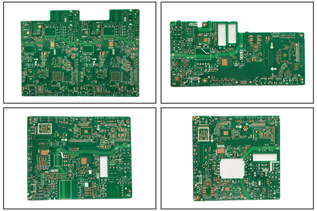
SAMPLE:
| ||||||||||||||||||||
| ||||||||||||||||||||
| Item | Details |
| Max layer count | 20 L |
| Max board thickness | 6.0 mm |
| Max aspect ratio | 10 : 1 |
| Max copper thickness | 6 OZ |
| Max dimension | 600 * 700mm |
| Min thickness of 4 layers PCB | 0.4 mm |
| Min hole / pad | 0.15 / 0.35mm |
| Hole location accuracy | + / - 0.05mm |
| PTH hole tolerance | + / - 0.05mm |
| Min line width and line space | 0.065 / 0.065mm |
| Surface treatment |
HASL / HASL lead free, OSP
Immersion gold/silver/tin, gold plating (hard gold and soft gold),
silver plating, tin plating, platinum plating, carbon ink,
ENEPIG (electroless nickel - electroless palladium - immersion gold) |
Lead Time
| Layer count | Sample lead time/workday | Batch lead time/workday |
| 1-2L | 2 | 6 |
| 4L | 5 | 8 |
| 6L | 5 | 9 |
| 8L | 6 | 10 |
| 10L | 8 | 10 |
| 12L | 8 | 12 |
| 14L | 10 | 15 |
| 16L | 10 | 18 |
| 18-40L (Up to difficulty) | at least 18 | at least 24 |
| P.S. For HDI, Blind/Buried Hole PCB: Regular Lead Time + 3 workdays | ||
-- We have spent massively on purchasing below advanced automated production equipments.
| Equipment Name | Plant in Shenzhen | Plant in Dongguan |
| CCD exposure machine | 8 | 12 |
| AOI test machine | 6 | 8 |
| Mechanical drilling rig | 26 | 53 |
| Automatic edge finishing machine | 2 | 2 |
| Pressing machine | 2 | 2 |
| VCP | 0 | 2 |
| Electroplating line | 1 | 2 |
| CNC routing machine | 12 | 12 |
| Automatic tester | 10 | 16 |
Now send us your inquiry, and you will be replied within 8 hours!
Little knowledge - Double Sided PCB
Double Sided PCBs also known as Double-Sided Plated Thru or DSPT,
which are the gateway to higher technology applications compared to
single sided PCB.
Double Sided PCB allow for the routing of traces around each other
by jumping between a top and bottom layer by way of vias.
The ability to cross paths from top to bottom greatly increasing
the circuit designer's flexibility in circuits designing and lends
itself to greatly increased circuit densities.


