

Active Member
|
[China]

Address: A1-405 (Exit A, Fuyong Metro Station), Fuhai Information Port, Bao'an District, Shenzhen. 10mins from Shenzhen Bao'an International Airport by subway
Contact name:Cyan Hong

Shenzhen Lefang Electronics Co., Ltd |
|
|
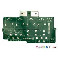
12 OZ Double Sided Thick Copper PCB Circuit Board with Lead Free HASL
The Thick Copper PCB Board is made with FR - 4 board raw material. And the copper thickness is 12 OZ / 420 µm while the board thickness 1.6 mm. And the specificaton of the heavy copper printed circuit board is 145*89 mm.

How to get quick quotation?
| Step 1 Please send us Gerber file with these format: .CAD / .Gerber / .PCB / .DXP / .P-CAD, etc | ||||||||||||||||||||
| Step 2 Also please provide us the below details for quick quotation: | ||||||||||||||||||||
Board material: Fr - 4 / CEM - 1 / CEM - 3 / 22F / Fr - 1 / others | ||||||||||||||||||||
| Material brand: SY / KB / Rogers (optional) | ||||||||||||||||||||
| Material Specification:High Tg / copper based / aluminum based or others (optional) | ||||||||||||||||||||
| Board thickness: 0.1 - 6.0 mm | ||||||||||||||||||||
| Copper thickness: 0.05 Oz - 8 Oz ( 17 um - 288 um ) | ||||||||||||||||||||
| Surface Treatment: OSP / ENIG / HASL / Lead Free HASL / Immersion Tin / Immersion Sin | ||||||||||||||||||||
| Color of solder mask and silk print: Green / red / blue / black / white / yellow ,etc | ||||||||||||||||||||
| Board size and quantity | ||||||||||||||||||||
If you don't have Gerber file, please provide us the imfomation as step 2 or post your PCB Board to us for clone.
| ||||||||||||||||||||
SAMPLE:
| ||||||||||||||||||||
| ||||||||||||||||||||
| Item | Details |
| Max layer count | 20 L |
| Max board thickness | 6.0 mm |
| Max aspect ratio | 10 : 1 |
| Max copper thickness | 6 OZ |
| Max dimension | 600 * 700mm |
| Min thickness of 4 layers PCB | 0.4 mm |
| Min hole / pad | 0.15 / 0.35mm |
| Hole location accuracy | + / - 0.05mm |
| PTH hole tolerance | + / - 0.05mm |
| Min line width and line space | 0.065 / 0.065mm |
| Surface treatment |
HASL / HASL lead free, OSP
Immersion gold/silver/tin, gold plating (hard gold and soft gold),
silver plating, tin plating, platinum plating, carbon ink,
ENEPIG (electroless nickel - electroless palladium - immersion gold) |
| Layer count | Sample lead time/workday | Batch lead time/workday |
| 1-2L | 2 | 6 |
| 4L | 5 | 8 |
| 6L | 5 | 9 |
| 8L | 6 | 10 |
| 10L | 8 | 10 |
| 12L | 8 | 12 |
| 14L | 10 | 15 |
| 16L | 10 | 18 |
| 18-40L (Up to difficulty) | at least 18 | at least 24 |
| P.S. For HDI, Blind/Buried Hole PCB: Regular Lead Time + 3 workdays | ||
| AOI (Automated Optical Inspection) | Impedance control |
| Automatic short-circuit testing | Metallographic microscope |
| RoHS detector | Fly probe/ fixture mold |
| Dielectric tester | Visual inspection |
Now send us your inquiry, and you will be replied within 8 hours!
Little knowledge - Thick copper PCB
Electronics are used in demanding environments and operate at higher currents in these days.
Thick copper PCB can help conduct heat away from components and withstand high current, satisfying the market of power conversion module boards which is used in automobile electronics and electric equipment.
Heavy copper PCBs means copper conductors 5 oz/ft2 – 19 oz/ft2 in inner and/or outer layers; sometimes defined as more than 4 oz per square foot (ft2).
These boards can be manufactured in a smaller footprint as they can contain multiple weights of copper on the same circuit layers.


