

Active Member
|
[China]

Address: NO.1 Industry Park, XinSheng Village, Longgang District, ShenZhen
Contact name:Frank

Shenzhen Found Printed Circuit Board Co., Ltd. |
|
|
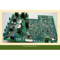
Custom-Made Multilayer PCBA Board immersion silver pcb ems pcb assembly
PCBA SMD SMT assembly
- ISO9001 certificated factory
- 0201 Chips, PLCC, BGA
- AOI inspection
- 100% visual check
-PCBA(Printed Circuit Board Assembly)for Telecom Control
Model NO.: FD-123
Dielectric: FR-4
Application: Medical Instruments
Mechanical Rigid: Rigid
Base Material: Copper
Brand: FD
Finished Copper Thickness: All 35um
Thickness Material: Rogers4350b
Soldermask Color: Green
PCB Testing: E-Testing, Flying Probe Testing
Lead Time: 9 Working Days
Transport Package: Vacuum Package
Origin: Shenzhen, China
Type: Rigid Circuit Board
Material: Fiberglass Epoxy
Flame Retardant Properties: V0
Processing Technology: Electrolytic Foil
Insulation Materials: Organic Resin
Layer Count: 6 Layers
Board Thickness: 1.6mm
Surface Finish: Enig
Specialities: Special Stackup,Rogers4350b
Ipc Standards: Ipc Class II
Trademark: FOUND
Specification: UL(US&Canada). ISO9001. RoHs, TS, SGS
HS Code: 8534009000
Our One-Stop Service for PCB & PCB Assembly manufacturing
We commit to offer high quality level circuit board(PCBA) to
customer
*Abundant experience and strong ability in material sourcing,
manufacturing, test and quality management
*Professional team in charge of product design
*Circuit boards 1 to 28 layers PCB layout, fabrication, PCB
assembly and box building
*High-precision 0201 size components SMT technology
*RoHS compaint SMT, DIP process
*High-precision E-Testing include: ICT in circuit, function test,
AOI, BGA repair device, etc
*Flexible production volume follow different customer requirement.
We offer quotation for clients within 3 working days, and reply
E-mail within 6 hours. Send us an inquiry today.
Product capability
| Seq | Item | capability |
| 1 | Base Material | FR-4, High TG FR-4 , Halogen Free material ,CEM-3,CEM-1,PTFE,Rogers ,Arlon ,Taconic,Aluminum base,Teflon,PI ,etc |
| 2 | Layers | 1-40 ( ≥30 layers needs review ) |
| 3 | Finished inner/outer copper thickness | 0.5-6OZ |
| 4 | Finished board thickness | 0.2-7.0mm(≤0.2mm needs review),≤0.4mm for HASL |
| Board thickness≤1.0mm: +/-0.1mm 1<Board thickness≤2.0mm: +/-10% Board thickness>2.0mm: +/-8% | ||
| 5 | Max panel size | ≤2sidesPCB: 600*1500mm Multilayer PCB: 500*1200mm |
| 6 | Min conductor line width/spacing | Inner layers: ≥3/3mil Outer layers: ≥3.5/3.5mil |
| 7 | Min hole size | Mechanical hole: 0.15mm Laser hole: 0.1mm |
| Drilling precision: first drilling First drilling: 1mil Second drilling: 4mil | ||
| 8 | Warpage | Board thickness≤0.79mm: β≤1.0% 0.80≤Board thickness≤2.4mm: β≤0.7% Board thickness≥2.5mm: β≤0.5% |
| 9 | Controlled Impedance | +/- 5 % Ω(<50Ω),+/-10%(≥50Ω),≥50Ω+/-5% (needs review) |
| 10 | Aspect Ratio | 15:01 |
| 11 | Min welding ring | 4mil |
| 12 | Min solder mask bridge | ≥0.08mm |
| 13 | Plugging vias capability | 0.2-0.8mm |
| 14 | Hole tolerance | PTH: +/-3mil NPTH: +/-2mil |
| 15 | Outline profile | Rout/ V-cut/ Bridge/ Stamp hole |
| 16 | Solder mask color | Green,yellow,black,blue,red,white,matte green |
| 17 | Component mark color | white,yellow,black |
| 18 | Surface treatment | OSP: 0.2-0.5um HASL: 2-40um Lead free HASL: 2-40um ENIG: Au 1-10U'' ENEPIG: PB 2-5U''/ Au 1-8U'' Immersion Tin:0.8-1.5um Immersion silver: 0.1-1.2um Peelable blue mask Carbon ink Gold plating: Au 1-150U'' |
| 19 | E-Test | Flying probe tester : 0.4-6.0mm,max 19.6*23.5inch |
| Min spacing from test pad to board edge : 0.5 mm | ||
| Min conductive resistance : 5 Ω | ||
| Max insulation resistance : 250 MΩ | ||
| Max test voltage : 500 V | ||
| Min test pad diameter : 6 mil | ||
| Min test pad to pad spacing : 10 mil | ||
| Max test current : 200 MA | ||
| 20 | AOI | Orbotech SK-75 AOI : 0.05-6.0mm,max 23.5*23.5inch |
| Orbotech Ves machine : 0.05-6.0mm,max 23.5*23.5inch |
FAQ
Q: What is the M.O.Q?
1pcs. printed circuit boards/pcb/pcba
Q: What file is needed for pcb quotation and fabrication?
- Gerber file of the bare PCB board is needed for pcb making; Bom list is also needed for pcb assembly.
- Quantity needed.
- Inspection method for PCB assembly if function test is required.
Q: What is the quotation time of pcb and pcba?
- PCB & FPC: within 1 hour
- PCBA: within 2 days
Q: Lead time of the precision pcb circuit board?
| Sample Lead time(days) | Mass production lead time(days) | |
| Single sided PCB | 1~3 | 4~7 |
| Double sided PCB | 2~5 | 7~10 |
| Multilayer PCB | 7~8 | 10~15 |
| PCB and Assembly | 8~15 | 15~30 |


