

Active Member
|
[China]

Address: NO.1 Industry Park, XinSheng Village, Longgang District, ShenZhen
Contact name:Frank

Shenzhen Found Printed Circuit Board Co., Ltd. |
|
|
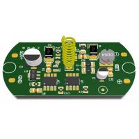
PCBA for Multilayer Printed Circuit Board with Prototype Circuit
Board
Introduction
Pls see our pcb catalog below:
1. single side pcb 2. double side pcb
3. Multilayer pcb(3-26+ layers) 4. Flexible PCB(FPC)
5. Rigid-flex PCB board 6. Aluminum PCB board for LED(1-4 layers)
7. MCPCB board (1-4 layers) 8.Ceramic PCB(1-4 layers)
9. HDI pcb board 10. High frequency PCB
11. PCB assembly
| PCB Description | Our PCB Board Capability | ||
| PCB Surface Finishes | electrolytic nickel-gold, HASL(Lead Free, ENIG (Electroless Nickel/Immersion Gold, Carbon Ink, Golden Fingers, OSP (Entek, Immersion Tin, Immersion Silver | ||
| PCB Max. Size | 1200mm×600mm | ||
| PCB Min. Size | 5mm×5 mm | ||
| Bow & Twist Tolerance | Single Side≤1.0%,Double Side≤0.7%, Muti-Layer≤0.5% | ||
| Min. Board Thickness & Tolerance | 0.2mm±0.08mm | ||
| PCB Min. trace/spacing | Tin board:0.2mm±20%(8mil±0%) | ||
| gold board:0.075mm±20%(3mil±0%) | |||
| Copper to Board Edge Spacing | 0.5mm(20mil) | ||
| Hole to Trace Spacing | 0.3mm(12mil) | ||
| Min. Hole Diameter | 0.2mm±.076mm(8mil±3mil) | ||
| Min. Hole Clearance | 0.4mm±.076mm(16mil±3mil) | ||
| Copper Thickness on Hole Wall | 20-25um(0.79mil-1.0mil) | ||
| Hole Location Tolerance | ±0.076mm(l±3mil) | ||
| Min Diameter of Punching Hole | FR-4 board thickness≤1.0mm(40mil):1.0mm(40mil) | ||
| FR-4 board thickness 1.2-3.0mm(48-120mil):1.5mm(60mil) | |||
| PCB Min. Punching Slot | FR-4 CEM-3 board thickness≤1. 0mm(40mil):0.8 mm×0.8 mm(32mil×32mil) | ||
| FR-4 board thickness1.2-3.0mm(48-120mil): 1.0 mm×1.0 mm(40mil×40mil) | |||
| Trace width variation | ±0.076mm(±3mil) | ||
| Outline Tolerance | Routing:±0.1mm (±4mil) ,Punching:±0.05mm (±2mil) | ||
| V-CUT Registration Tolerance±0.2mm (±8mil) | |||
| PCB BOARD Type | Single-sided, double-sided, multi-layer | ||
| Major Material | FR-4, CEM-1,CEM-3, high frequency laminates, Aluminum, NiFe-based, copper base | ||
| PCB BOARD Thickness | 0.2-3.5mm | ||
| Base Copper Thickness | 11um 35um 70um 105um | ||
| Max. aspect ratio(board thickness: hole size) | 8:1 | ||
| V-Cut Angle Tolerance | ±5° | ||
| V-Cut Board Thickness | 0.4mm -3.2mm(16mil -128mil) | ||
| Min SMT Pitch | 0.3mm(12mil) | ||
| Min. Component mark | 0.15mm(6mil) | ||
| Min. width of annular ring(finished) | 0.15mm(6mil)/side | ||
| Min pad opening | 0.076mm(3mil) | ||
| Min S/M Bridge | ±0.076mm(±3mil) | ||
| carbon ink board manufacturing capability:1.Impedance Control:20K±10% 2.Hardness:6H 3.bearable friction times :above 200000 times | |||
| Technology | |||
| Min trace/space(inner/external) | 3/3 mil0.075/0.075mm | ||
| Min drill size for through hole | drill 8.0 mil0.20mm | ||
| Laser dill | 4 mil0.1mm | ||
| Copper Foil Thickness | 17-210um | ||
| Inner Core Thickness | ±0.08mm | ||
| Tolerance of total board thickness | ±0.015mm | ||
| Max .Unit Area | 700-800 | ||
| Min. Unit Area | 2-5mm | ||
| Max Layer | 1-18 Layers | ||
| Surface Treatment | |||
| Solder Coating Thickness Sn | 4-20um | ||
| Cobalt/ Gold plating, Hard Gold Thickness | Ni:5-10umAu:0.05-0.20um | ||
| Gold/Nickel Plating Thickness | Ni:5-10umAu:0.05-0.15um | ||
| OSP Coating Thickness | 0.2-0.5um | ||
| Electroness Au Thickness | Ni:3-15umAu:0.025-0.10mm | ||
| Chem .Tin Thickness | Sn:0.8-5um | ||
| Producting Capacity | each day :800-100m2 | ||
| Aspect Ratio | 6:01:00 | ||
| Hole Registration | 0.004" (0.1mm) | ||
Trade Terms:
1. Payment: T/T in advance (Western Union , payple is welcomed)
2. Production lead time 100PCS: 5-7days, 500~1000PCS: 7-10days,
above 1000PCS 15-20days.
3. Sample can be delivered in 3days
4. Shipping freight are quoted under your requests
5. Shipping port: Shen zhen,Mainland China
6. Discounts are offered based on order quantities
7. MOQ: 1PCS
Package &Shipping Methods:
1.Vacuum package with silica gel, Carton box with packing belt.
2. By DHL, UPS, FedEx, TNT
3. By EMS (Usually for Russia Clients)
4. By sea for mass quantity according to customer's requirement


