Active Member
|
[China]

Address: NO.1 Industry Park, XinSheng Village, Longgang District, ShenZhen
Contact name:Frank

Shenzhen Found Printed Circuit Board Co., Ltd. |
|
|
Quick Details
Place of Origin: Guangdong, China
Brand Name:FOUND
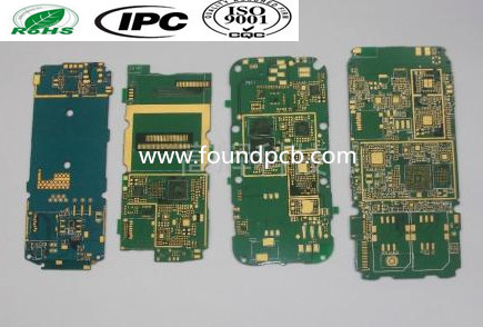
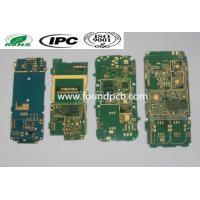
Model Number: Multi-Layer Enig Gold Finger PCB copper plating pcb copper circuit board
Base Material: FR4, FR4/High TG FR-4/M4/ M6/Rogers/Nelco/Isola
Copper Thickness: 1oz
Board Thickness: 1.6mm
Min. Hole Size: 0.1mm
Min. Line Width: 3mil
Min. Line Spacing: 3mil
Surface Finishing: ENIG,HASL,OSP,ENEPIG
Keywords: pcb circuit boards
PCB Standard: IPC-A-600
Solder Mask: Green,Black,Blue,Red,Matt Green
Legend: White,Black,Red,Yellow
Product quotation: Within 2 Hours
Service: 24Hours technical services
Sample delivery: Within 24 Hours
Our PCB board manufacture and PCB assembly service:
1. No MOQ for PCB and PCBA
2. High standard pcb depends on IPC Class ll
3. 100% E-tested guarantee before shipping
4. RoHS, UL, ISO, SGS certificate approved
5. Factory production Capability of 10000 sqm/month
Testing Procedures For PCB Board: ---We perform multiple quality assuring procedures before shipping out any PCB board. These include:
* Visual Inspection
* Flying probe, fixture tool
* Impedance control
* Solder-ability detection
* Digital metallograghic microscope
* AOI (Automated Optical Inspection)
Product capability
| Seq | Item | capability |
| 1 | Base Material | FR-4, High TG FR-4 , Halogen Free material ,CEM-3,CEM-1,PTFE,Rogers ,Arlon ,Taconic,Aluminum base,Teflon,PI ,etc |
| 2 | Layers | 1-40 ( ≥30 layers needs review ) |
| 3 | Finished inner/outer copper thickness | 0.5-6OZ |
| 4 | Finished board thickness | 0.2-7.0mm(≤0.2mm needs review),≤0.4mm for HASL |
| Board thickness≤1.0mm: +/-0.1mm 1<Board thickness≤2.0mm: +/-10% Board thickness>2.0mm: +/-8% | ||
| 5 | Max panel size | ≤2sidesPCB: 600*1500mm Multilayer PCB: 500*1200mm |
| 6 | Min conductor line width/spacing | Inner layers: ≥3/3mil Outer layers: ≥3.5/3.5mil |
| 7 | Min hole size | Mechanical hole: 0.15mm Laser hole: 0.1mm |
| Drilling precision: first drilling First drilling: 1mil Second drilling: 4mil | ||
| 8 | Warpage | Board thickness≤0.79mm: β≤1.0% 0.80≤Board thickness≤2.4mm: β≤0.7% Board thickness≥2.5mm: β≤0.5% |
| 9 | Controlled Impedance | +/- 5 % Ω(<50Ω),+/-10%(≥50Ω),≥50Ω+/-5% (needs review) |
| 10 | Aspect Ratio | 15:01 |
| 11 | Min welding ring | 4mil |
| 12 | Min solder mask bridge | ≥0.08mm |
| 13 | Plugging vias capability | 0.2-0.8mm |
| 14 | Hole tolerance | PTH: +/-3mil NPTH: +/-2mil |
| 15 | Outline profile | Rout/ V-cut/ Bridge/ Stamp hole |
| 16 | Solder mask color | Green,yellow,black,blue,red,white,matte green |
| 17 | Component mark color | white,yellow,black |
| 18 | Surface treatment | OSP: 0.2-0.5um HASL: 2-40um Lead free HASL: 2-40um ENIG: Au 1-10U'' ENEPIG: PB 2-5U''/ Au 1-8U'' Immersion Tin:0.8-1.5um Immersion silver: 0.1-1.2um Peelable blue mask Carbon ink Gold plating: Au 1-150U'' |
| 19 | E-Test | Flying probe tester : 0.4-6.0mm,max 19.6*23.5inch |
| Min spacing from test pad to board edge : 0.5 mm | ||
| Min conductive resistance : 5 Ω | ||
| Max insulation resistance : 250 MΩ | ||
| Max test voltage : 500 V | ||
| Min test pad diameter : 6 mil | ||
| Min test pad to pad spacing : 10 mil | ||
| Max test current : 200 MA | ||
| 20 | AOI | Orbotech SK-75 AOI : 0.05-6.0mm,max 23.5*23.5inch |
| Orbotech Ves machine : 0.05-6.0mm,max 23.5*23.5inch |
Advantages
1, High thermal conductivity
2, Excellent thermal diffusivity
3, Good electrical insulation
4, Products can be of smaller size by removing radiator parts.
5, High withstand voltage of metal base material is up to 4500V.
Q1. Can I have a sample order to test It?
A: Yes, we welcome sample order to test and check quality. Mixed
samples are acceptable.
Q2. What about the lead time?
A: Sample needs 3-5 days; mass production time needs 8-12 days.
Q3. Do you have MOQ for all PCBs?
A: NO MOQ, we do custom made flexible PCB, depends on customers' projects.
Q4. How do you ship the goods and how long does It take to arrive?
A: For small quantity, we ship it by DHL, UPS, FedEx or TNT. It usually takes 3-5 days, and for big quantity needs 20-30 days by sea (the detail will be confirmed with the forwarder).
Q5. I have no drawing, how to process It?
A: Firstly, let us know your detail requirements (if you have sample, please ship to us, we will copy it).
Secondly, we quote according to your requirements or our suggestions.
Thirdly, customer confirms the samples and places deposit for formal order.
Fourthly, we arrange the production.
Q6. Is It OK to print my logo on product?
A: Yes. Please inform us formally before our production and confirm the design firstly based on our sample.