Active Member
|
[China]

Address: NO.1 Industry Park, XinSheng Village, Longgang District, ShenZhen
Contact name:Frank

Shenzhen Found Printed Circuit Board Co., Ltd. |
|
|
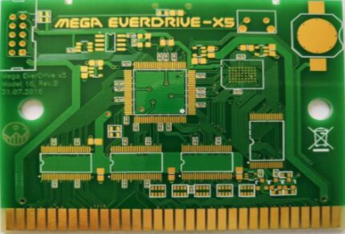
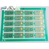
0.2MM PLATNG EDGE 6 layer copper thickness pcb 4 oz copper pcb
Quick Details
Place of Origin:Guangdong, China
Brand Name:FOUND
Model Number:rigid board
Copper Thickness:0.5-2oz
Board Thickness:0.1-0.5mm
Min. Hole Size:0.1-6.5mm
Min. Line Width:3mil
Min. Line Spacing:3mil
Surface Finishing:ENIG,HASL,OSP,ENEPIG,Flash Gold
Keywords:heavy copper pcb
Max Layer:8L
Product quotation:Within 2 Hours
PCB Standard:IPC-A-600
Sample delivery:Within 24 Hours
Service:24Hours technical services
Solder Mask:Green Solder Mask/Black PI/Yellow PI
Legend:White,Black,Red,Yellow
Our One-Stop Service for PCB & PCB Assembly manufacturing
1. Quick Quotation - Competitive factory direct price is always
offered
2. Free Sample - Sample for free before mass production
3. Quality Control - Complete test procedure is necessary
4. On Time Delivery - Customize the logistics plan according to
customer's requirement
5. After-sale Service - Reply to the claim within 24 hours to make
sure our customer's manufacturing
Product capability
| Seq | Item | capability |
| 1 | Base Material | FR-4, High TG FR-4 , Halogen Free material ,CEM-3,CEM-1,PTFE,Rogers ,Arlon ,Taconic,Aluminum base,Teflon,PI ,etc |
| 2 | Layers | 1-40 ( ≥30 layers needs review ) |
| 3 | Finished inner/outer copper thickness | 0.5-6OZ |
| 4 | Finished board thickness | 0.2-7.0mm(≤0.2mm needs review),≤0.4mm for HASL |
| Board thickness≤1.0mm: +/-0.1mm 1<Board thickness≤2.0mm: +/-10% Board thickness>2.0mm: +/-8% | ||
| 5 | Max panel size | ≤2sidesPCB: 600*1500mm Multilayer PCB: 500*1200mm |
| 6 | Min conductor line width/spacing | Inner layers: ≥3/3mil Outer layers: ≥3.5/3.5mil |
| 7 | Min hole size | Mechanical hole: 0.15mm Laser hole: 0.1mm |
| Drilling precision: first drilling First drilling: 1mil Second drilling: 4mil | ||
| 8 | Warpage | Board thickness≤0.79mm: β≤1.0% 0.80≤Board thickness≤2.4mm: β≤0.7% Board thickness≥2.5mm: β≤0.5% |
| 9 | Controlled Impedance | +/- 5 % Ω(<50Ω),+/-10%(≥50Ω),≥50Ω+/-5% (needs review) |
| 10 | Aspect Ratio | 15:01 |
| 11 | Min welding ring | 4mil |
| 12 | Min solder mask bridge | ≥0.08mm |
| 13 | Plugging vias capability | 0.2-0.8mm |
| 14 | Hole tolerance | PTH: +/-3mil NPTH: +/-2mil |
| 15 | Outline profile | Rout/ V-cut/ Bridge/ Stamp hole |
| 16 | Solder mask color | Green,yellow,black,blue,red,white,matte green |
| 17 | Component mark color | white,yellow,black |
| 18 | Surface treatment | OSP: 0.2-0.5um HASL: 2-40um Lead free HASL: 2-40um ENIG: Au 1-10U'' ENEPIG: PB 2-5U''/ Au 1-8U'' Immersion Tin:0.8-1.5um Immersion silver: 0.1-1.2um Peelable blue mask Carbon ink Gold plating: Au 1-150U'' |
| 19 | E-Test | Flying probe tester : 0.4-6.0mm,max 19.6*23.5inch |
| Min spacing from test pad to board edge : 0.5 mm | ||
| Min conductive resistance : 5 Ω | ||
| Max insulation resistance : 250 MΩ | ||
| Max test voltage : 500 V | ||
| Min test pad diameter : 6 mil | ||
| Min test pad to pad spacing : 10 mil | ||
| Max test current : 200 MA | ||
| 20 | AOI | Orbotech SK-75 AOI : 0.05-6.0mm,max 23.5*23.5inch |
| Orbotech Ves machine : 0.05-6.0mm,max 23.5*23.5inch |
About us
Shenzhen Found provides 1~32layers(include 1~8oz copper thickness PCB and HDI) PCB and PCB assembly services to a wide range of companies in the Consume , Computer, Industrial, RF products, Automotive, Securities, medical, Telecommunications and other electronics equipment markets. As a full service turnkey supplier of custom electronics, FOUNDcan provide support from design and prototyping to new product introduction and full rate production. The main idea of running this business is to locate any potential customers around the world and extensively supplying them with good quality PCBs and related assembly services.
How to get quick quotation?
Step 1. Please send us Gerber file with these format: .CAD/
.Gerber/ .PCB / .DXP/ .P-CAD, etc;
Step 2. Also please provide us the below details for quick
quotation:
a) Board material: Fr-4/ CEM-1/ CEM-3/ SY/ KB/ Rogers/High Tg/
copper based/ aluminum based, etc;
b) Board thickness: 0.1-6.0mm;
c) Copper thickness: 0.05 Oz-8Oz (17um-288um)
d) Surface Treatment: OSP/ ENIG/ HASL/ Lead Free HASL/ Immersion
Tin/ Immersion Sin
e) Color of solder mask and silk print: Green/ red/ blue/ black/
white/ yellow
f) Board size and quantity
g) BOM(Bill of Materials) list if PCB Assembly