Active Member
|
[China]

Address: 4113-4116# A Area, HSST PARK, BAO'AN District, Shenzhen, China
Contact name:Wendy

Abis Circuits Co., Ltd. |

|
|
6 Layer HDI PCB, Immersion Gold Fr4 TG170 Multilayer Printed Circuit Board in Blue Ink
What is a HDI PCB?
IPC-2226 defines HDI as a printed circuit board with a higher wiring density per unit area than conventional printed circuit boards (PCB). They have finer lines and spaces ≤ 100 µm / 0.10mm, smaller vias (<150 µm) and capture pads <400 µm / 0.40mm, and higher connection pad density (>20 pads/cm2) than employed in conventional PCB technology.
Product We Produce:
1. Rigid, Flex, Rigid-Flexible PCB.
2. Buried/Blind Vias, Via in Pad, Counter Sink Hole, Screw
Hole(Counterbore), Press-fit, Half Hole.
3. HASL lead-free, Immersion Gold/ Silver/Tin, OSP, Gold
plating/finger, Peelable mask,
4. Printed Circuit Boards adhere to IPC Class 2 & 3
international PCB standard.
5. Quantities range from prototype to medium & big batch
production.
6. 100% E-test
Multilayer HDI PCB Production Range:
| Number of layers | 4 – 22 layers standard, 30 layers advanced |
| Technology highlights | Multilayer boards with a higher connection pad density than standard boards, with finer lines/spaces, smaller via holes and capture pads allowing microvias to only penetrate select layers and also be placed in surface pads. |
| HDI builds | 1+N+1, 2+N+2, 3+N+3,4+N+4, any layer in R&D |
| Materials | FR4 standard, FR4 high performance, Halogen free FR4, Rogers |
| Copper weights (finished) | 18μm – 70μm |
| Minimum track and gap | 0.075mm / 0.075mm |
| PCB thickness | 0.40mm – 3.20mm |
| Maxmimum dimensions | 610mm x 450mm; dependant upon laser drilling machine |
| Surface finishes available | OSP, ENIG, Immersion tin, Immersion silver, Electrolytic gold, Gold fingers |
| Minimum mechanical drill | 0.15mm |
| Minimum laser drill | 0.10mm standard, 0.075mm advanced |
Testing:
E-testing | 100% |
QFP Pitch | 16mil (0.40mm) |
BGA Pitch | 16mil (0.40mm) |
Connector Pitch | 16mil (0.40mm) |
AOI | All Multilayer |
Impedance Control | ± 10% |
Solderability Testing | As standard |
Ionic Contamination | On Request |
Why choose us:
1, With ABIS, customers significantly and effectively reduce their
global procurement costs. Behind each service provided by ABIS, is
hidden a cost saving for customers.
2, We have two shop together, one is for prototype, quick turn,
small volume making. The other is for mass production also for HDI
board, with highly skilled professional employees, for high quality
products with competitive price and on-time delivery.
3, We provide very professional sales, technical and logistic
supports, on a world-wide basis.hours complaint feedback
Lead Time:
| Number of Layers | Quick Turn Lead Time |
| 2 | 24 Hours |
| 4 | 48 Hours |
| 6 | 72 Hours |
| 8 | 96 Hours |
| 10 | 120 Hours |
| 12 | 120 Hours |
| 14 | 144 Hours |
| 16 | Depend on Technical Specification |
| 18 | Depend on Technical Specification |
| 20 | Depend on Technical Specification |
Our mission:
PCBs for demanding customers, on time with zero defects, produced
sustainably at the lowest total cost. Manufacturing many different
types of PCBs in smaller series (High-mix, Low-volume) involves
constantly adjusting, adapting and problem solving.
Our responsibility:
We know that the PCB is a critical key component for our customers.
And we know for sure that anything can happen during the complex
production process involved – and it often does. In our world,
taking full responsibility means a lot of things, including a
responsible and sustainable approach in everything we do –
socially, environmentally and ethically. When a problem occurs, we
try as hard as we can to understand the problem and find a
solution. Our mindset is that we own the problem and don’t leave
until we have cleared it up.
Delivery Time:
Air Freight Lead Time – 4 Days |
Sea Freight Lead Time – 30 Days |
All Far East lead times are subject to customs clearance |
Premium International shipments can be arranged by DHL, Fedex, UPS or TNT at extra cost |
FAQ :
Q1: How can I got quotation:
A: Please send gerber file with format: .PCB / .P-CAD / .DXP / .CAD / .Gerber
Q2: Do you have pcb in stock?
A: Most of our pcb board are customised, which according to gerber
file.
ABIS have sample in stock could sent to you for a quality checking
always.
Q3: What board manufacturer do you use for FR4?
A: Main Suppliers(FR4): Kingboard (Hong Kong), NanYa (Taiwan) and
Shengyi (China).
Q4: Will my PCB files be checked?
A: Checked within 12 hours. Once Engieer question and working file
checked, production will start.
Q5: What do you require in order to produce an assembly quotation?
A: Bill of materials (BOM) detailing:
a), manufacturers parts numbers ,
b), components suppliers' parts number (e.g. Digi-key, Mouser, RS )
c), PCBA sample photos if possible.
d), Quantity
Q6: Does ABIS CIRCUITS bevel gold fingers?
A: Yes. A standard 45-degree bevel, also bevel at 15 or 30 degrees
upon request. For multi-layer board, please ensure there is
adequate back set forthe bevels.
Q7: My assembly company need the PCBs as panelized, can you do this
for me?
A: Yes. We can panelize your circuits upon your request.
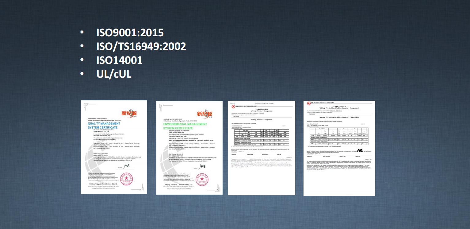
Certifications:
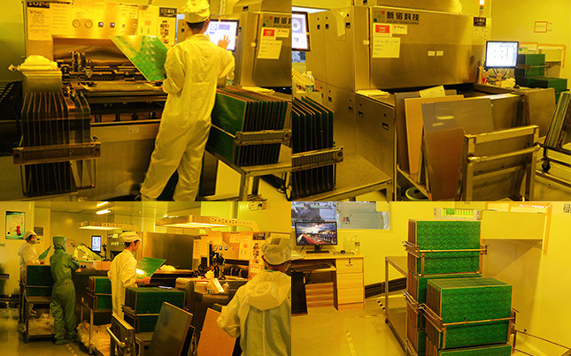
Work Shop:

Customer Visit: