Active Member
|
[China]

Address: Room 201 Building A2 Industrial Park No. 6 Yuanchuang Park Rongfu road, Fucheng Street Longhua District Shenzhen City 518131
Contact name:Sandy

Shenzhen Shinelink Technology Ltd |
|
|
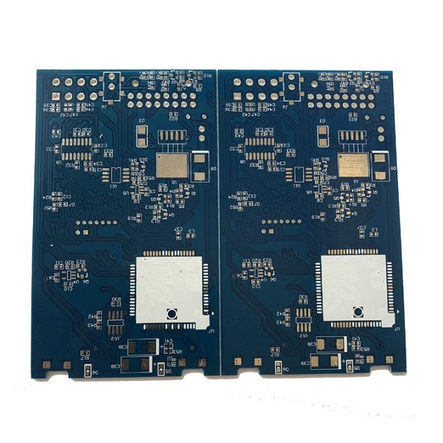
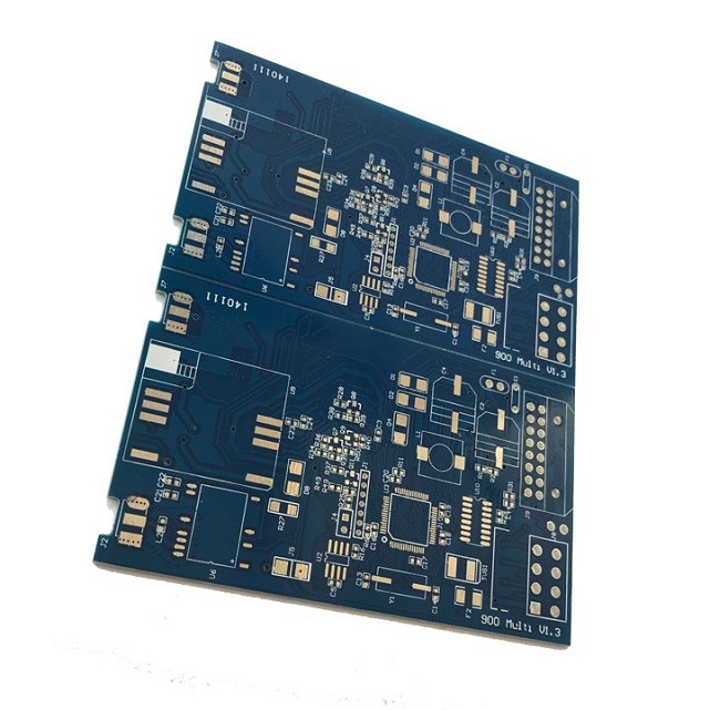
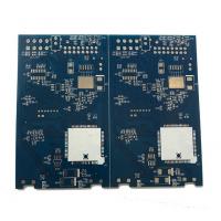
Multilayer PCB Board prototype 10 layers electronic circuit board
Multilayer 10 layers PCB board
The high technology as a starting point,the use of first-class equipment and raw material production and sales of high precision ,high density multi-layer LCD as our products and technology development direction,build up the company:"linePossess first-class PCB enterprise"as our vision ,to provide high quality electronic information industry PCB production Satisfactory products and sincere service" as our mission.
Advantages
- No MOQ
- OEM services provided
- Heavy copper PCB, Heavy gold PCB, Blind / Buried via PCB, High layer count PCB manufacturable
- Factory direct price
- Replying with price in one working day
- Shipping within 24 hours
- Certificate: ROHS, UL, ISO9001-2000, ISO14001,SGS Lead-Free
PCB Capacity
PCB General Capability | |
Number of Layer | 1 - 18 Layer |
Maximum Processing Area | 680 × 1000MM |
Min Board Thickness | 2 Layer - 0.3MM ( 12 mil ) |
4 Layer - 0.4MM ( 16 mil ) | |
6 Layer - 0.8MM ( 32 mil ) | |
8 Layer - 1.0MM ( 40 mil) | |
10 Layer - 1.1MM ( 44 mil ) | |
12 Layer - 1.3MM ( 52 mil ) | |
14 Layer - 1.5MM ( 59 mil ) | |
16 Layer - 1.6MM ( 63 mil ) | |
18 Layer - 1.8MM ( 71 mil ) | |
Finished Board Thickness Tolerance | Thickness ≤ 1.0MM, Tolerance: ± 0.1MM |
1.0MM ≤ Thickness ≤ 6.5MM, Tolerance ± 10% | |
Twisting and Bending | ≤ 0.75%, Min: 0.5% |
Range of TG | 130 - 215 ℃ |
Impedance Tolerance | ± 10%, Min: ± 5% |
Hi-Pot Test | Max: 4000V/10MA/60S |
Surface Treatment | HASL, With Lead, HASL Free Lead |
Flash Gold, Immersion Gold | |
Immersion Silver, Immersion Tin | |
Gold Finger, OSP | |
PCB Cu Thickness + Plating | |
Out Layer Cu Thickness | 1 - 6OZ |
Inner Layer Cu Thickness | 0.5 - 4OZ |
Cu Thickness of PTH | 20UM ≤ Average ≤ 25UM |
Min: 18UM | |
HASL with Lead | Tin 63% Lead 37% |
HASL Free Lead | 7UM ≤ Surface Thickness ≤ 12UM |
Thick Gold Plating | Ni Thickness: 3 - 5UM ( 120u" - 200u" ) |
Gold Thickness: 0.025 - 1.27UM ( 1u" - 50u" ) | |
Immersion Gold | Ni Thckness: 3 - 5UM ( 120u" - 200u" ) |
Gold Thickness: 0.025 - 0.15UM ( 1u" - 3u" ) | |
Immersion Silver | Ag Thickness: 0.15- 0.75 UM ( 6u" - 30u" ) |
Gold Finger | Ni Thickness: 3 - 5UM ( 120u" - 160u" ) |
Gold Thickness: 0.025 - 1.51UM ( 1u" - 60u" ) | |
U940 PCB Pattern Limit Capability |
|
Min Width | 0.075MM ( 3 mil ) |
Min Trace | 0.075MM ( 3 mil ) |
Min Width of Ring ( Inner Layer ) | 0.15MM ( 6 mil ) |
Min Width of Ring ( Out Layer ) | 0.1MM ( 4 mil ) |
Min Solder Bridge | 0.1MM ( 4 mil ) |
Min Height of Legend | 0.7MM ( 28 mil ) |
Min Width of Legend | 0.15MM ( 6 mil ) |
PCB Holes Processing Capability | |
Final Hole Size | Min: Laser 0.1MM, Machine 0.2MM |
Drilling Hole Size | 0.10 - 6.5MM |
Drilling Tolerance | NPTH: ±0.05MM, PTH: ±0.075MM |
Final Hole Size Tolerance ( PTH ) | φ0.20 - 1.60MM ± 0.075MM |
φ1.60 - 6.30MM ± 0.10MM | |
Final Hole Size Tolerance ( NPTH ) | φ0.20 - 1.60MM ± 0.05MM |
φ1.60 - 6.50MM ± 0.05MM | |
Drilling Strip Hole | -0L ~tu.'gth /width 2:1 |
Min Strip Hole Width 0.65MM | |
Length & Width Tolerance ± 0.05MM | |
Board Thickness / Hole Size | ≤ 10:1 |
PCB Cover Thickness Capability | |
Solder Mask Color | Green,Matte Green,Yellow,Blue,Red,Black,Matte Black,White |
Solder Mask Thickness | Surface Line ≥ 10UM |
Surface Line Corner ≥ 6UM | |
Surface Board 10 - 25UM | |
Solder Mask Bridge Width | |
Legend Color | White,Yellow,Black |
Min Height of Legend | 0.70MM ( 28 mil ) |
Min Width of Legend | 0.15MM ( 6 mil ) |
Blue Gel Thickness | 0.2 - 1.5MM |
Blue Gel Tolerance | ±0.15MM |
Carbon Print Thickness | 5 - 25UM |
Carbon Print Min Space | 0.25MM |
Carbon Print Impedance | 200Ω |
Blind/Burried/Half Via PCB Capability |
|
Parameters | (1+1)e.g. (4-layer)blind via:1-2,2-4 (6-layer)buried via:2-3,3-4 (8-layer)blind/buried:1-3,4-5,6-8 |
Min Via | Laser 0.1MM, Machine 0.2MM |
Half Via | Min: 0.6MM |
Impedance Capability | |
Resistance Value | Single-ended 50 - 75Ω, Difference 100Ω, Coplanar 50 - 75Ω |
PCB Photos