

Active Member
|
[China]

Address: Room 201 Building A2 Industrial Park No. 6 Yuanchuang Park Rongfu road, Fucheng Street Longhua District Shenzhen City 518131
Contact name:Sandy

Shenzhen Shinelink Technology Ltd |
|
|
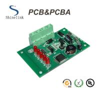
Elevator One stop pcba board with components sourcing , 2 OZ PC Board Assembly
More professional service, more concessions!
Shinelink company is more than just a leading PCBA manufacturer, We provide high quality pcb assembly services to customers worldwide. With expertise in printed circuit board (PCB) assembly, Shinelink has grown to become a one-stop PCBA manufacturer for complete PCB assembly services.
Files Requested For PCB Assembly Quotation
---In order to provide you with the most efficient and accurate
quote on manufacturing the requested unit, we ask that you provide
us with the following information.
1. Gerber file,PCB file,Eagle file or CAD file are all acceptable
2. A detailed bill of materials (BOM)
3. Clear pictures of PCB or PCBA sample for us
4. Quantity and delivery required
5. Test method for PCBA to guarantee 100% good quality products.
6. Schematics file for PCB design if need to do function test.
7. A sample if available for better sourcing
8. CAD files for enclosure manufacturing if required
9. A complete wiring and assembly drawing showing any special
assembly instructions if required
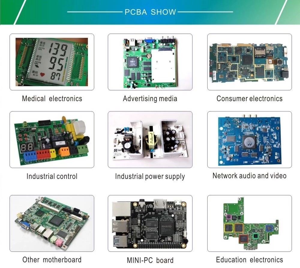
Shinelink kinds PCBA Products
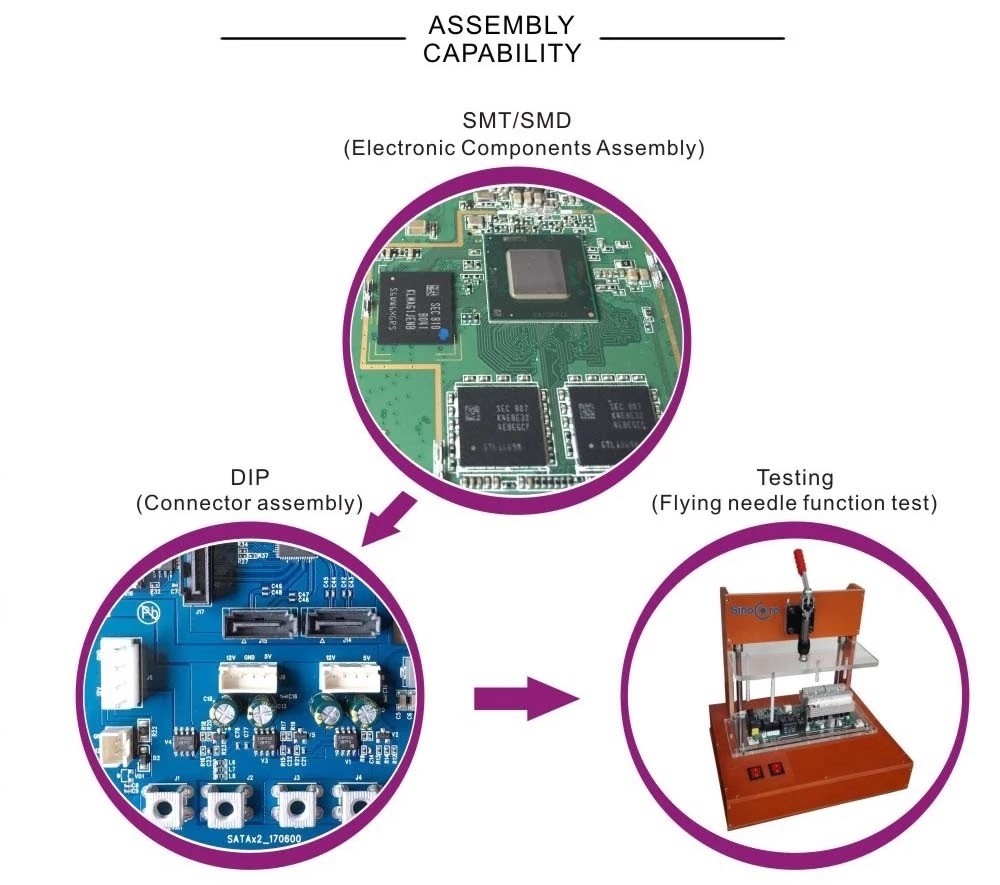
PCB Assembly Capabilities
| Turnkey PCBA | PCB+components sourcing+assembly+package |
| Assembly details | SMT and Thru-hole, ISO lines |
| Lead Time | Prototype: 15 work days. Mass order: 20~25 work days |
| Testing on products | Flying Probe Test, X-ray Inspection, AOI Test, functional test |
| Quantity | Min quantity: 1pcs. Prototype, small order, mass order, all OK |
| Files we need | PCB: Gerber files(CAM, PCB, PCBDOC) |
| Components: Bill of Materials(BOM list) | |
| Assembly: Pick-N-Place file | |
| PCB panel Size | Min size: 0.25*0.25 inches(6*6mm) |
| Max size: 20*20 inches(500*500mm) | |
| PCB Solder Type | Water Soluble Solder Paste, RoHS lead free |
| Components details | Passive Down to 0201 size |
| BGA and VFBGA | |
| Leadless Chip Carriers/CSP | |
| Double-sided SMT Assembly | |
| Fine Pitch to 0.8mils | |
| BGA Repair and Reball | |
| Part Removal and Replacement | |
| Component package | Cut Tape,Tube,Reels,Loose Parts |
| PCB assembly process | Drilling-----Exposure-----Plating-----Etaching &
Stripping-----Punching-----Electrical Testing-----SMT-----Wave
Soldering-----Assembling-----ICT-----Function
Testing-----Temperature & Humidity Testing |
FAQ
1. How do O-Leading ensure quality?
Our high quality standard is achieved with the following.
1.1 The process is strictly controlled under ISO 9001:2008
standards.
1.2 Extensive use of software in managing the production process
1.3 State-of-art testing equipments and tools. E.g. Flying Probe,
X-ray Inspection, AOI (Automated Optical Inspector) and ICT
(in-circuit testing).
1.4.Dedicated quality assurance team with failure case analysis
process
1.5.Continuous staff training and education
2. How do O-Leading keep your price competitive?
Over the last decade, prices of many raw materials (e.g. copper, chemicals) had doubled, tripled or quadrupled; Chinese currency RMB had appreciated 31% over US dollar; And our labor cost also increased significantly.
However, O-Leading have kept our pricing steady. This owns entirely to our innovations in reducing cost, avoiding wastes and improving efficiency. Our prices are very competitive in the industry at the same quality level.
We believe in a win-win partnership with our customers. Our partnership will be mutually beneficial if we can provide you an edgeon cost and quality.
3. What kinds of boards can O-Leading process?
Common FR4, high-TG and halogen-free boards, Rogers, Arlon, Telfon, aluminum/copper-based boards, PI, etc.
4. What data are needed for PCB & PCBA production?
4.1 BOM (Bill of Materials) with reference designators: component
description, manufacturer’s name and part number.
4.2 PCB Gerber files.
4.3 PCB fabrication drawing and PCBA assembly drawing.
4.4 Test procedures.
4.5 Any mechanical restrictions such as assembly height
requirements.
5. What’s the typical process flow for multi-layer PCB?
Material cutting → Inner dry film → inner etching → Inner AOI → Multi-bond→ Layer stack up Pressing → Drilling → PTH → Panel Plating → Outer Dry Film → Pattern Plating → Outer etching → Outer AOI → Solder Mask → Component Mark → Surface finish → Routing → E/T → Visual Inspection.


