

Active Member
|
Address: 7/F, High-Tech Park, Shangkeng Community, Guanlan Subdist., Baoan District, Shenzhen, Guangdong, China (Mainland)
Contact name:

Shen Zhen Xu Xin Technology Co., Ltd. |
|
|
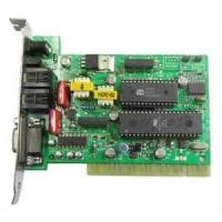
OEM Multilayer PCBA, 10 Layer printed circuit board PCB Assembly for controller
RoHS OEM PCB Assembly SMY/DIP
1.PCB Layout,PCB design
2.Make high difficulty PCB(1-38 layers boards)
3.offer all Electric components
4.ISO9001/TS16949/ROHS
5.PCB delivery time:5-10 days; PCBA delivery time:20-25 days
We are professional manufacturer in various PCB and PCBA with many years experience,We can provide a reasonable price with high quality products.
* 1. PCB layout, PCB design
* 2: Make high difficulty PCB(1 to 38 layers)
* 3: Provide all Electronic component
* 4: PCB assembly
* 5: Write programs for clients
* 6: PCBA/finished product Test. etc.
1.PCB Specification detail.
2.Details for PCB Assembly
Technical
1).Professional surface mounting and through hole soldering technology;
2).Various sizes,like 1206,0805,0603 components SMT technology;
3).ICT(In Circuit Test),FCT(Functional Circuit Test) technology;
4).Nitrogen gas reflow soldering technology for SMT;
5).High standard SMT&Solder Assembly line;
6).High density interconnected board placement technology capacity.
Quote requirement
1).The detailed files(Gerber files,specification and BOM);
2).Clear pictures of PCBA or samples for us;
3).PCBA Test method.