

Active Member
|
[China]

Address: 3418, Duhuixuan, Shennan Avenue, Futian District, Shenzhen, Guangdong Province, China
Contact name:段

Shenzhen Hongxinwei Technology Co., Ltd |
|
|
W25Q80DVSSIG NOR Flash spiFlash, 8M-bit, 4Kb Uniform Sector
1.GENERAL DESCRIPTION
The W25Q80DV/DL (8M-bit) Serial Flash memory provides a storage
solution for systems with limited space, pins and power. The 25Q
series offers flexibility and performance well beyond ordinary
Serial Flash devices. They are ideal for code shadowing to
RAM,executing code directly from Dual/Quad SPI(XIP)andstoring
voice, text and data. The W25Q80DV operates on a single 2.7V to
3.6V and the W25Q80DL operateds on a single 2.3V to 3.6Vpower
supply with current consumption as low as 1μ A for power-down.
The W25Q80DV/DLarray is organized into 4,096 programmable pages of
256-bytes each. Up to 256 bytes can be programmed at a time. Pages
can be erased ingroups of 16 (4KB sector erase), groups of 128
(32KB block erase), groups of 256 (64KB block erase) or the entire
chip (chip erase). The W25Q80DV/DLhas 256 erasable sectors and 16
erasable blocks respectively. The small 4KB sectors allow for
greater flexibility in applications that require data and parameter
storage.
The W25Q80DV supports the standard Serial Peripheral Interface
(SPI), and a high performance Dual/Quad output as well as Dual/Quad
I/O SPI: Serial Clock, Chip Select, Serial Data I/O0 (DI), I/O1
(DO), I/O2 (/WP), and I/O3 (/HOLD). SPI clock frequencies of up to
104MHz are supported allowing equivalent clock rates of 208MHz
(104MHz x 2) for Dual I/O and 416MHz (104MHz x 4) for Quad I/O when
using the Fast Read Dual/Quad I/O instructions. These transfer
rates can outperform standard Asynchronous 8 and 16-bit Parallel
Flash memories. A Hold pin, Write Protect pin and programmable
write protection,with top, bottom or complement array
control,provide further control flexibility. Additionally, the
device supports JEDEC standard manufacturer and device
identification with a 64-bit Unique Serial Number.
2.FEATURES
Family of SpiFlash Memories
–W25Q80DV/DL: 8M-bit/1M-byte (1,048,576)–256-byte per programmable
page–Standard SPI: CLK,/CS,DI,DO,/WP,/Hold–Dual SPI:CLK,/CS, IO0,
IO1, /WP, /Hold–Quad SPI:CLK,/CS, IO0, IO1, IO2, IO3–Uniform 4KB
Sectors, 32KB & 64KB Blocks
Highest Performance Serial Flash
–W25Q80DV104MHz Dual/Quad SPI clocks208/416MHz equivalent Dual/Quad
SPI50MB/S continuous data transfer rate–W25Q80DL80MHz Dual/Quad SPI
clocks160/320MHz equivalent Dual/Quad SPI40MB/S continuousdata
transfer rate
Software and Hardware Write Protection–Write-Protect all or portion
of memory–Enable/Disable protection with /WP pin–Top or bottom
array protection
Flexible Architecture with 4KB sectors–Uniform Sector/Block Erase
(4/32/64-kbytes)–Erase/Program Suspend & Resume–More than
100,000 erase/write cycles
Low Power, Wide Temperature Range
–W25Q80DV:Single 2.7 to 3.6V supply–W25Q80DL:Single 2.3to 3.6V
supply–<1μA Power-down(typ.)
Advanced Security & Identification Features
–Software and Hardware Write-Protect–Top/Bottom, 4KB complement
array protection–Power Supply Lock-Down and OTP protection–64-Bit
Unique ID for each device–Discoverable Parameters
(SFDP)Register–3X256-Byte Security Registers with OTP
locks–Volatile & Non-volatile Status Register Bits
3..PACKAGE TYPES AND PIN CONFIGURATIONS
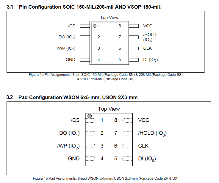
4.Pin Configuration PDIP 300-mil

5.Ball Configuration WLCSP

6.4.1Chip Select (/CS)The SPI Chip Select (/CS) pin enables and
disables device operation. When /CSis high the device is deselected
and the Serial Data Output (DO, or IO0, IO1, IO2, IO3) pins are at
high impedance. When deselected, the devices power consumption will
be at standby levels unless an internal erase, program or write
status register cycle is in progress. When /CSis brought low the
device will be selected, power consumption will increase to active
levels and instructions can be written to and data read from the
device. After power-up, /CSmust transition from high to low before
a new instruction will be accepted. The /CS input must track the
VCC supply level at power-up (see “Power-up Timing and Write
inhibit threshold” and figure 45). If needed,a pull-up resister on
/CS can be used to accomplish this.
4.2Serial Data Input, Output and IOs (DI, DO and IO0, IO1, IO2,
IO3)TheW25Q80DV/DLsupport standard SPI, Dual SPI and Quad SPI
operation. Standard SPI instructions use the unidirectional DI
(input) pin to serially write instructions, addresses or data to
the device on the rising edge of the Serial Clock (CLK) input pin.
Standard SPI also uses the unidirectional DO (output) to read data
or status from the device on the falling edge of CLK.Dual and Quad
SPI instructions use the bidirectional IO pins to serially write
instructions, addresses or data to the device on the rising edge of
CLK and read data or status from the device on the falling edge of
CLK. Quad SPI instructions require the non-volatile Quad Enable bit
(QE) in Status Register2 to be set. When QE=1, the /WP pin becomes
IO2 and /HOLD pin becomes IO3.
4.3Write Protect (/WP)The Write Protect (/WP) pin can be used to
prevent the Status Register from being written. Used in conjunction
with the Status Register’s Block Protect (CMP, SEC, TB, BP2, BP1
and BP0)bits and Status Register Protect(SRP0)bits, a portion as
small as 4KBsector or the entire memory array can be hardware
protected. The /WP pin is active low. When the QE bit of Status
Register-2 is set for Quad I/O, the /WP pin function is not
available since this pin is used for IO2.
4.4HOLD (/HOLD)The /HOLD pin allows the device to be paused while
it is actively selected. When /HOLD is brought low, while /CSis
low, the DO pin will be at high impedance and signals on the DI and
CLK pins will be ignored (don’t care). When /HOLD is brought high,
device operation can resume. The/HOLDfunction can be useful when
multiple devices are sharing the same SPI signals. The /HOLD pin is
active low. When the QE bit of Status Register-2 is set for Quad
I/O, the /HOLD pin function is not available since this pin is used
for IO3. See figure 1a and 1b for the pin configuration of Quad I/O
operation
4.5Serial Clock (CLK)The SPI Serial Clock Input (CLK) pin provides
the timing for serial input and output operations.
7.Why choose us?
100% new and originao with Advantage price
High efficiency
Fast Delivery
Professional team service
10 Years Experience Electronic components
Electronic components Agent
Advantage logistic discount
Excellent After-sales Service


