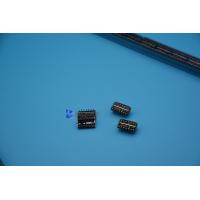
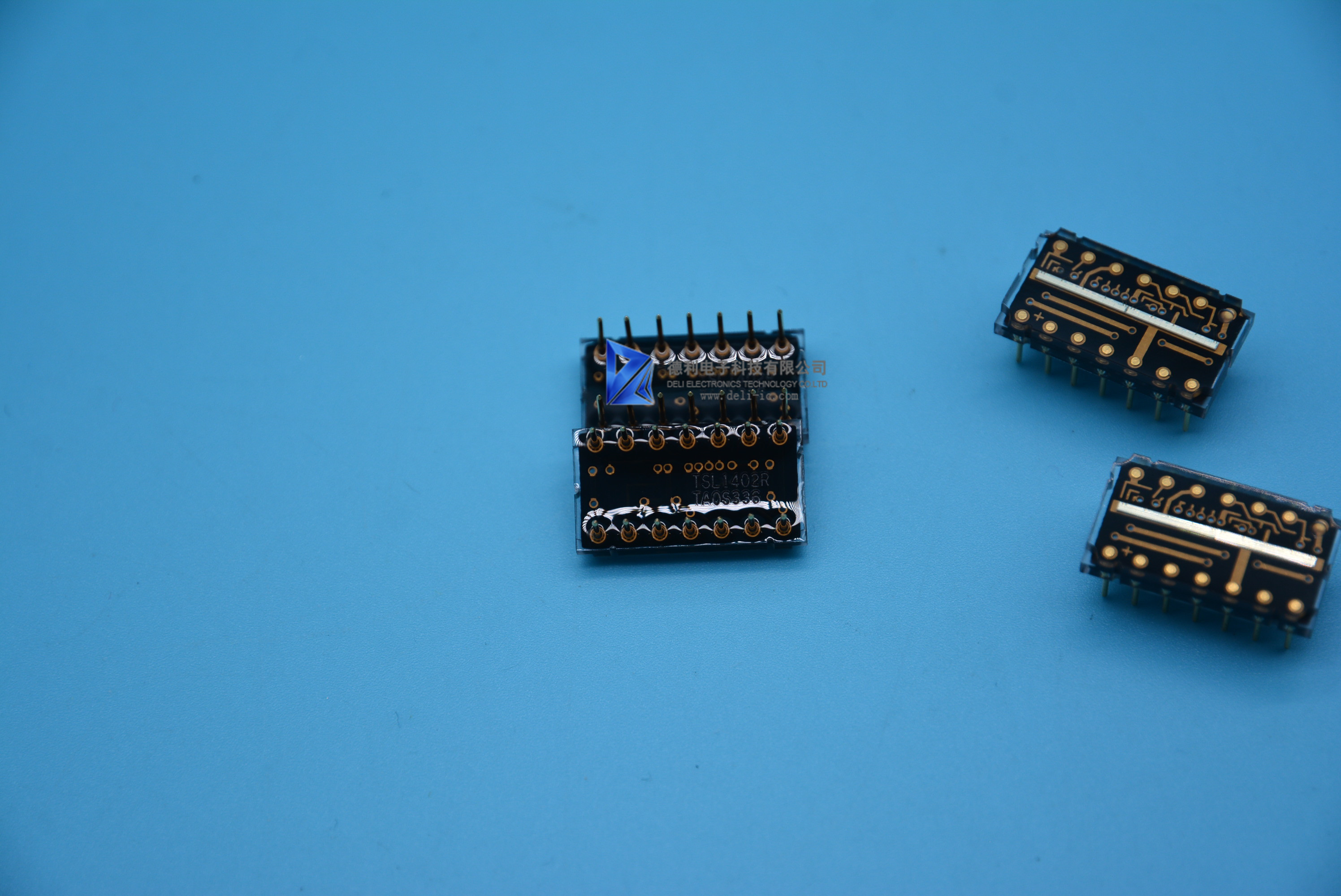
TSL1402R # 256 × 1 Linear Sensor Array With Hold DIP14
Linear Sensor Array 256X1
NC − No internal connection:
256 × 1 Sensor-Element Organization
400 Dots-Per-Inch (DPI) Sensor Pitch
High Linearity and Uniformity
Wide Dynamic Range . . . 4000:1 (72 dB)
Output Referenced to Ground
Low Image Lag ... 0.5% Typ
Operation to 8 MHz
Single 3-V to 5-V Supply
Rail-to-Rail Output Swing (AO)
No External Load Resistor Required
Replacement for TSL1402
Description:
The TSL1402R linear sensor array consists of two sections of 128
photodiodes each and associated charge
amplifier circuitry, aligned to form a contiguous 256 × 1 pixel
array. The device incorporates a pixel data-hold
function that provides simultaneous integration start and stop
times for all pixels. The pixels measure 63.5 μm
by 55.5 μm, with 63.5-μm center-to-center spacing and 8-μm spacing
between pixels. Operation is simplified
by internal logic requiring only a serial-input pulse (SI) and a
clock.
The TSL1402R is intended for use in a wide variety of applications
including mark and code reading, OCR and
contact imaging, edge detection and positioning, and optical
encoding
MECHANICAL INFORMATION:
This assembly consists of 2 sensor chips mounted on a
printed-circuit board in a clear molded plastic package.
Notes:
A. All linear dimensions are in millimeters.
B. The true-position spacing is 2.54 mm between lead centerlines.
Each pin centerline is located within 0.25 mm of its true
longitudinal positions.
C. Index of refraction of clear plastic is 1.52.
D. The gap between the individual sensor dies in the array is 57 μm
typical (51 μm minimum and 75 μm maximum).
E. This drawing is subject to change without notice.
THEORETICAL PIXEL LAYOUT FOR IDEAL CONTINUOUS DIE
ACTUAL MULTI-DIE PIXEL LAYOUT FOR DIE-TO-DIE EDGE JOINING
Notes 2:
A. All linear dimensions are in micrometers.
B. Spacing between outside pixels of adjacent die is typical.
C. Die-to-die spacing.
D. This drawing is subject to change without notice.
Figure 12. Edge Pixel Layout Dimensions
Production Data :
— information in this document is current at publication date.
Products conform to specifications in accordance with the terms of
Texas Advanced Optoelectronic Solutions, Inc. standard
warranty.
Production processing does not necessarily include testing of all
parameters.
Deli electronics tehcnology Co.,Ltd
http://www.icmemorychip.com/
Email:sales3@deli-ic.com
Skype:hkdeli881
Contact: VIVI-CHEN