

Active Member
|
[China]

Address: Room 301, Building 1, Shahu Science and Technology Park, SIP, SUZHOU City,Jiangsu Province,P.R.C
Contact name:Jerry He

Topmatch Electronics (Suzhou) Co., Limited. |
|
|
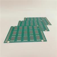
0.3pitch 8Layer HDI PCBs for Burn in boards and semiconductor Test boards / thin board
A burn-in board is a printed circuit board that is used in the burn-in process.
The components added to the board are stressed using extreme heat to highlight any failures. Once the stress tests have been completed engineers will analyse the results to make sure everything is working within the correct parameters.
During the burn-in process extreme temperatures often ranging from 125°C – 250°C or even 300°C are applied so the materials used need to be extremely durable. Generally speaking we use IS410 for applications up to 155°C and polyimide for applications up to 250°C. For temperatures over 250°C a higher grade of polyimide is used. We also use high temperature lead free solders and stainless-steel board fixtures.
1 . Descriptions:
What is a BIB ?
A burn-in board is a printed circuit board that is used in the burn-in process. The components added to the board are stressed using extreme heat to highlight any failures. Once the stress tests have been completed engineers will analyse the results to make sure everything is working within the correct parameters.
2 . Specifications:
| Name | 0.3pitch 8Layer HDI PCBs for Burn in boards and semiconductor Test boards |
| Number of Layers | 8 |
| Quality Grade | IPC 6012 Class 2,IPC 6012 Class 3 |
| Material | IT180 |
| Thickness | 0.8mm |
| Min Track/Spacing | 75um/75um |
| Min Hole Size | Laser 75um |
| Solder Mask | Green |
| Silkscreen | White |
| Surface Finish | Immersion gold + OSP |
| Finished Copper | 12um |
| Production time | 10-21 working days |
| Lead time | 2-3 days |


