

Active Member
|
[China]

Address: Room 301, Building 1, Shahu Science and Technology Park, SIP, SUZHOU City,Jiangsu Province,P.R.C
Contact name:Jerry He

Topmatch Electronics (Suzhou) Co., Limited. |
|
|
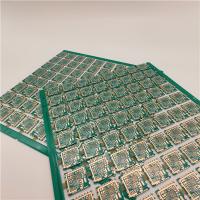
94v0 Circuit Mp3 Pcb 3.5mm Audio Jack Pcb 94v 0 Pcb Board
PCBs that run high-tech electronics tend to have several layers. Of course, boards that are composed of more than one layer, or one with components on two sides will cost more than a single-layer board. PCBs need several components, which is why they need so many layers stacked upon each other. When boards are bigger, they cost more than the smaller ones. The space that the components consume increases the cost of the PCBs. The price increases not just because the PCBs are bigger; this is because bigger boards and boards with several layers take more time to manufacture.
| PCB Item | Manufacture Capacity |
| Layer Counts | 1--20L |
| Base Material | FR4,High-TG FR4,CEM3,aluminum,High Frequency(Rogers,Taconic,Aron,PTFE,F4B) |
| Material Thickness(mm) | 0.40, 0.60, 0.80, 1.00, 1.20, 1.50, 1.60, 2.0, 2.4, 3.2 |
| Max board size(mm) | 1200x400mm |
| Board Outline Tolerance | ±0.15mm |
| Board Thickness | 0.4mm--3.2mm |
| Thickness Tolerance | ±8% |
| Minimum line/space | 0.1mm |
| Min Annular Ring | 0.1mm |
| SMD Pitch | 0.3mm |
| Holes | |
| Min Hole Size(mechanical) | 0.2mm |
| Min Hole Size(laser hole) | 0.1mm |
| Hole Size Tol (+/-) | PTH:±0.075mm;NPTH: ±0.05mm |
| Hole Position Tol | ±0.075mm |
| Plating | |
| HASL/LF HAL | 2.5um |
| Immersion Gold | Nickel 3-7um Au:1-5u'' |
| Surface Finish | HAL,ENIG,Plated Gold,Immersion Gold,OSP |
| Copper | |
| Copper Weight | 0.5--6oz |
| Color | |
| Solder mask | Green, Blue, Black, White, Yellow, Red, Matt Green, Matt Black, Matt Blue |
| Silk screen | White, Black, Blue,Yellow |
| Acceptable File Format | Gerber file,Powerpcb,CAD,AUTOCAD,ORCAD,P-CAD,CAM-350,CAM2000 |
| Certificate | ROSH,ISO9001,UL |
1. How to design a Hybrid multilayer PCB ?
Multilayer printedcircuit boards (PCBs) can provide many advantages to RF/microwave circuit designers in terms of achieving high functional density in a small size, while also improving reliability and cutting cost. As some designers have found, the multiple layers need not be the same dielectric materials: a growing number of RF/ microwave circuit designs are being implemented with hybrid multilayer PCBs, in which different materials are used among the layers. This allows the choice of materials to be tailored to the various functions on the different layers of the PCB. Of course, there are some areas of concern when adopting such a design approach, and this article will provide a simple overview of these hybrid multilayer PCBs in terms of fabrication, electrical performance, and the types of circuit materials that are suitable for hybrid multilayer PCBs.
One circuit material that is used quite often in high-frequency hybrid multilayer PCBs is FR-4, although it may not be the most ideal choice for some circuits. Low-cost FR-4 circuit materials have been in use for a wide range of circuits for decades. FR-4 is glass-reinforced epoxy laminate material. Its performance is predictable and reliable, and it can be processed with basic fabrication methods. However, FR-4 exhibits a very high dissipation factor, which translates into high dielectric losses for circuits at microwave frequencies. Because of its loss characteristics, FR-4 is typically not used for pure RF/microwave circuits, but has been used in some high-frequency hybrid multilayer PCBs for various reasons. FR-4 is available in standard grade and with high glass transition temperature (Tg), which is the temperature at which the modulus of the material will change dramatically. Such temperature changes can impact the reliability of plated through holes (PTHs) through the laminate, as used to interconnect different circuit layers in a multilayer PCB. Some high-Tg FR-4 materials provide good stability with the processing temperatures required for many circuit fabrication techniques, with relatively low coefficient of thermal expansion (CTE) in the z-axis for good PTH reliability.
Hybrid multilayer PCBs often make use of circuit materials with very different values of dielectric constant (Dk). For example, some multilayer antenna circuits may consist of a low-Dk circuit material as the outside layer for radiating elements, a moderate-Dk circuit material internally for a stripline antenna feed line, and a high-Dk material for an internal layer for filter circuitry. The different Dk materials are often based on different resin systems. The outer, low-Dk layer may be PTFE material while the inner, moderateDk circuit layer is formed on a ceramic-filled hydrocarbon-based laminate. The bonding materials could be based on either type of material, although hydrocarbonbased bonding materials are more often used for their ease of circuit fabrication.
2. Product application
Printed circuit boards (PCBs) with characteristic impedance control are widely used in high frequency circuit. PCB's that mixed high frequency material can reduce signal loss at high frequencies and meet the development needs of communication technology.
It is mainly used in the infrastructure field of transmission cores including WDM/OTN end-to-end intelligent optical transmission platform, MSTP/multi-service transmission platform, microwave fusion transmission radio frequency, data communication system platform, and other information communication industries.


