

Active Member
|
[China]

Address: #506B, Henghui Business Center, No.77, Lingxia Nan Road, High Technology Zone, Huli, Xiamen 361006, China
Contact name:

XIAMEN POWERWAY ADVANCED MATERIAL CO., LTD. |
|
|
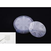
A Plane N-GaN Freestanding GaN Substrate
PAM-XIAMEN has established the manufacturing technology for freestanding (Gallium Nitride)GaN substrate wafer which is for UHB-LED and LD. Grown by hydride vapour phase epitaxy (HVPE) technology,Our GaN substrate has low defect density and less or free macro defect density.
PAM-XIAMEN offers full range of GaN and Related III-N Materials including GaN substrates of various orientations and electrical conductivity,crystallineGaN&AlN templates, and custom III-N epiwafers.
Here Shows Detail Specification:
A Plane N-GaN Freestanding GaN Substrate
| Item | PAM-FS-GaN A-N |
| Dimension | 5 x 10 mm2 |
| Thickness | 350 ±25 µm 430±25 µm |
| Orientation | A plane (11-20) off angle toward M-axis 0 ±0.5° A plane (11-20) off angle toward C-axis -1 ±0.2° |
| Conduction Type | N-type |
| Resistivity (300K) | < 0.5 Ω·cm |
| TTV | ≤ 10 µm |
| BOW | -10 µm ≤ BOW ≤ 10 µm |
| Surface Roughness: | Front side: Ra<0.2nm, epi-ready; Back side: Fine Ground or polished. |
| Dislocation Density | From 1 x 10 5to 5 x 106 cm-2 |
| Macro Defect Density | 0 cm-2 |
| Useable Area | > 90% (edge exclusion) |
| Package | each in single wafer container, under nitrogen atmosphere, packed in class 100 clean room |
A Plane N-GaN Freestanding GaN Substrate
PAM-XIAMEN's GaN(Gallium Nitride) substrate is singlecrystal substrate with high quality, which is made with original HVPE method and wafer processing technology. They are high crystalline, good uniformity, and superior surface quality. GaN substrates are used for many kinds of applications, for white LED and LD(violet, blue and green), Furthermore development has progressed for power and high frequency electronic device applications.
GaN is a very hard (12±2 GPa, mechanically stable wide bandgap semiconductor material with high heat capacity and thermal conductivity. In its pure form it resists cracking and can be deposited in thin film on sapphire or silicon carbide, despite the mismatch in their lattice constants. GaN can be doped with silicon (Si) or with oxygen to n-type and with magnesium (Mg) to p-type. However, the Si and Mg atoms change the way the GaN crystals grow, introducing tensile stresses and making them brittle.Galliumnitride compounds also tend to have a high dislocation density, on the order of 108 to 1010 defects per square centimeter. The wide band-gap behavior of GaN is connected to specific changes in the electronic band structure, charge occupation and chemical bond regions.
Zinc Blende crystal structure
| Remarks | Referens | ||
| Energy gaps, Eg | 3.28 eV | 0 K | Bougrov et al. (2001) |
| Energy gaps, Eg | 3.2 eV | 300 K | |
| Electron affinity | 4.1 eV | 300 K | |
| Conduction band | |||
| Energy separation between Γ valley and X valleys EΓ | 1.4 eV | 300 K | Bougrov et al. (2001) |
| Energy separation between Γ valley and L valleys EL | 1.6 ÷ 1.9 eV | 300 K | |
| Effective conduction band density of states | 1.2 x 1018 cm-3 | 300 K | |
| Valence band | |||
| Energy of spin-orbital splitting Eso | 0.02 eV | 300 K | |
| Effective valence band density of states | 4.1 x 1019 cm-3 | 300 K |
 | Band structure of zinc blende(cubic) GaN. Important minima of the conduction band and maxima of the valence
band. 300K; Eg=3.2 eVeV; EX= 4.6 eV; EL= 4.8-5.1 eV; Eso = 0.02 eV For details see Suzuki, Uenoyama & Yanase (1995) . |
 | Brillouin zone of the face centered cubic lattice, the Bravais lattice of the diamond and zincblende structures. |


