

Active Member
|
[China]

Address: #506B, Henghui Business Center, No.77, Lingxia Nan Road, High Technology Zone, Huli, Xiamen 361006, China
Contact name:

XIAMEN POWERWAY ADVANCED MATERIAL CO., LTD. |
|
|
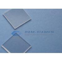
High-Purity M Plane N-GaN Freestanding GaN(Gallium Nitride) Substrate
PAM-XIAMEN has established the manufacturing technology for freestanding (Gallium Nitride)GaN substrate wafer which is for UHB-LED and LD. Grown by hydride vapour phase epitaxy (HVPE) technology,Our GaN substrate has low defect density and less or free macro defect density.
PAM-XIAMEN offers full range of GaN and Related III-N Materials including GaN substrates of various orientations and electrical conductivity,crystallineGaN&AlN templates, and custom III-N epiwafers.
Here Shows Detail Specification:
M Plane N-GaN Freestanding GaN Substrate
| Item | PAM-FS-GaN M-N |
| Dimension | 5 x 10 mm2 |
| Thickness | 350 ±25 µm 430 ±25 µm |
| Orientation | M plane (1-100) off angle toward A-axis 0 ±0.5° M plane (1-100) off angle toward C-axis -1 ±0.2° |
| Conduction Type | N-type |
| Resistivity (300K) | < 0.05 Ω·cm |
| TTV | ≤ 10 µm |
| BOW | -10 µm ≤ BOW ≤ 10 µm |
| Surface Roughness | Front side: Ra<0.2nm, epi-ready; Back side: Fine Ground or polished. |
| Dislocation Density | From 1 x 10 5to 5 x 10 6cm-2 |
| Macro Defect Density | 0 cm-2 |
| Useable Area | > 90% (edge exclusion) |
| Package | each in single wafer container, under nitrogen atmosphere, packed in class 100 clean room |
Application of GaN Substrate
Solid State Lighting:GaN devices are used as ultra high brightness light emitting diodes (LEDs), TVs, automobiles, and general lighting
DVD Storage: Blue laser diodes
Power Device: GaN devices are used as various components in high-power and high-frequency power electronics like cellular base stations, satellites, power amplifiers, and inverters/converters for electric vehicles (EV) and hybrid electric vehicles (HEV). GaN’s low sensitivity to ionizing radiation (like other group III nitrides) makes it a suitable material for spaceborne applications such as solar cell arrays for satellites and high-power, high-frequency devices for communication, weather, and surveillance satellites
Wireless Base Stations: RF power transistors
Wireless Broadband Access: high frequency MMICs,RF-Circuits MMICs
Pressure Sensors:MEMS
Heat Sensors: Pyro-electric detectors
Power Conditioning: Mixed signal GaN/Si Integration
Automotive Electronics: High temperature electronics
Power Transmission Lines: High voltage electronics
Frame Sensors: UV detectors
Solar Cells:GaN’s wide band gap covers the solar spectrum from 0.65 eV to 3.4 eV (which is practically the entire solar spectrum), making indium gallium nitride
(InGaN) alloys perfect for creating solar cell material. Because of this advantage, InGaN solar cells grown on GaN substrates are poised to become one of the most important new applications and growth market for GaN substrate wafers.
Ideal for HEMTs, FETs
GaN Schottky diode project: We accept custom spec of Schottky diodes fabricated on the HVPE-grown, free-standing gallium nitride (GaN) layers of n- and p-types.
Both contacts (ohmic and Schottky) were deposited on the top surface using Al/Ti and Pd/Ti/Au.
Surface Roughness-GaN material-TEST REPORT
A test report is necessary to show the compliance between custom description and our final wafers data. We will test the wafer characerization by equipment before shipment, testing surface roughness by atomic force microscope, type by Roman spectra instrument, resistivity by non-contact resistivity testing equipment,micropipe density by polarizing microscope, orientation by X-ray Orientator etc. if the wafers meet the requirement, we will clean and pack them in 100 class clean room, if the wafers do not match the custom spec, we will take it off.
Surface roughness is usually shortened to roughness and is a component of surface texture. It is quantified by the deviation of the normal vector direction of the real surface from its ideal form. If these deviations are large, the surface is rough; If they’re small, the surface is smooth. In surface measurement, roughness is generally considered to be the high frequency short-wave length component of measuring scale surface. In practice, however, it is often necessary to know the amplitude and frequency to ensure that the surface is suitable for a purpose.
Below is an example of surface roughness of GaN material:

A surface roughness-gan
 Substrate")
 Substrate")
 Substrate")
 Substrate")
 Substrate")
 Substrate")