

Active Member
|
[China]

Address: #506B, Henghui Business Center, No.77, Lingxia Nan Road, High Technology Zone, Huli, Xiamen 361006, China
Contact name:

XIAMEN POWERWAY ADVANCED MATERIAL CO., LTD. |
|
|
A Plane U-GaN Freestanding Hvpe-GaN Substrate For Iii-Nitride Devices
PAM-XIAMEN has established the manufacturing technology for freestanding (Gallium Nitride)GaN substrate wafer which is for UHB-LED and LD. Grown by hydride vapour phase epitaxy (HVPE) technology,Our GaN substrate has low defect density and less or free macro defect density.
PAM-XIAMEN offers full range of GaN and Related III-N Materials including GaN substrates of various orientations and electrical conductivity,crystallineGaN&AlN templates, and custom III-N epiwafers.
Here Shows Detail Specification:
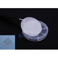
A Plane U-GaN Freestanding GaN Substrate
| Item | PAM-FS-GaN A-U |
| Dimension | 5 x 10 mm2 |
| Thickness | 350 ±25 µm 430±25 µm |
| Orientation | A plane (11-20) off angle toward M-axis 0 ±0.5° A plane (11-20) off angle toward C-axis -1 ±0.2° |
| Conduction Type | N-type |
| Resistivity (300K) | < 0.1 Ω·cm |
| TTV | ≤ 10 µm |
| BOW | -10 µm ≤ BOW ≤ 10 µm |
| Surface Roughness: | Front side: Ra<0.2nm, epi-ready; Back side: Fine Ground or polished. |
| Dislocation Density | From 1 x 10 5to 5 x 106 cm-2 |
| Macro Defect Density | 0 cm-2 |
| Useable Area | > 90% (edge exclusion) |
| Package | each in single wafer container, under nitrogen atmosphere, packed in class 100 clean room |
A Plane U-GaN Freestanding GaN Substrate
PAM-XIAMEN's GaN(Gallium Nitride) substrate is singlecrystal substrate with high quality, which is made with original HVPE method and wafer processing technology. They are high crystalline, good uniformity, and superior surface quality. GaN substrates are used for many kinds of applications, for white LED and LD(violet, blue and green), Furthermore development has progressed for power and high frequency electronic device applications.
GaN is a very hard (12±2 GPa, mechanically stable wide bandgap semiconductor material with high heat capacity and thermal conductivity. In its pure form it resists cracking and can be deposited in thin film on sapphire or silicon carbide, despite the mismatch in their lattice constants. GaN can be doped with silicon (Si) or with oxygen to n-type and with magnesium (Mg) to p-type. However, the Si and Mg atoms change the way the GaN crystals grow, introducing tensile stresses and making them brittle.Galliumnitride compounds also tend to have a high dislocation density, on the order of 108 to 1010 defects per square centimeter. The wide band-gap behavior of GaN is connected to specific changes in the electronic band structure, charge occupation and chemical bond regions.
Lattice constant of GaN substrate
Lattice parameters of gallium nitride were measured using high‐resolution x‐ray diffraction
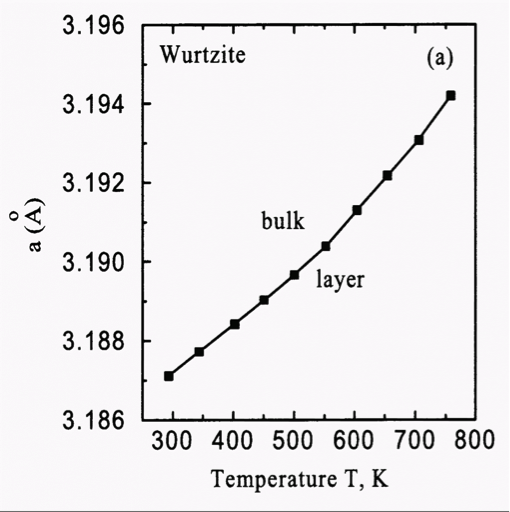
GaN,Wurtzite sructure. The lattice constants a vs. temperature.
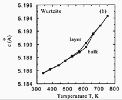
GaN,Wurtzite sructure. The lattice constants c vs. Temperature
Properties of GaN substrate
| PROPERTY / MATERIAL | Cubic (Beta) GaN | Hexagonal (Alpha) GaN |
| . | . | . |
| Structure | Zinc Blende | Wurzite |
| Space Group | F bar4 3m | C46v ( = P63mc) |
| Stability | Meta-stable | Stable |
| Lattice Parameter(s) at 300K | 0.450 nm | a0 = 0.3189 nm c0 = 0.5185 nm |
| Density at 300K | 6.10 g.cm-3 | 6.095 g.cm-3 |
| Elastic Moduli at 300 K | . . . | . . . |
| Linear Thermal Expansion Coeff. | . . . | Along a0: 5.59x10⁻⁶ K-1 Along c0: 7.75x10⁻⁶ K-1 |
| at 300 K | ||
| Calculated Spontaneous Polarisations | Not Applicable | – 0.029 C m-2 Bernardini et al 1997 Bernardini & Fiorentini 1999 |
| Calculated Piezo-electric Coefficients | Not Applicable | e33 = + 0.73 C m-2 e31 = – 0.49 C m-2 Bernardini et al 1997 Bernardini & Fiorentini 1999 |
| Phonon Energies | TO: 68.9 meV LO: 91.8 meV | A1(TO): 66.1 meV E1(TO): 69.6 meV E2: 70.7 meV A1(LO): 91.2 meV E1(LO): 92.1 meV |
| Debye Temperature | 600K (estimated) Slack, 1973 | |
| Thermal Conductivity near 300K | . . . | Units: Wcm-1K-1 1.3, Tansley et al 1997b 2.2±0.2 for thick, free-standing GaN Vaudo et al, 2000 2.1 (0.5) for LEO material where few (many) dislocations Florescu et al, 2000, 2001 circa 1.7 to 1.0 for n=1x10¹⁷ to 4x1018cm-3 in HVPE material Florescu, Molnar et al, 2000 2.3 ± 0.1 in Fe-doped HVPE material of ca. 2 x10⁸ ohm-cm, & dislocation density ca. 105 cm-2 (effects of T & dislocation density also given). Mion et al, 2006a, 2006b |
| Melting Point | . . . | . . . |
| Dielectric Constant at Low/Lowish Frequency | . . . | Along a0: 10.4 Along c0: 9.5 |
| Refractive Index | 2.9 at 3eV Tansley et al 1997b | 2.67 at 3.38eV Tansley et al 1997b |
| Nature of Energy Gap Eg | Direct | Direct |
| Energy Gap Eg at 1237K | 2.73 eV Ching-Hua Su et al, 2002 | |
| Energy Gap Eg at 293-1237 K | 3.556 - 9.9x10⁻⁴T2 / (T+600) eV Ching-Hua Su et al, 2002 | |
| Energy Gap Eg at 300 K | 3.23 eV Ramirez-Flores et al 1994 . 3.25 eV Logothetidis et al 1994 | 3.44 eV Monemar 1974 . 3.45 eV Koide et al 1987 . 3.457 eV Ching-Hua Su et al, 2002 |
| Energy Gap Eg at ca. 0 K | 3.30 eV Ramirez-Flores et al1994 Ploog et al 1995 | 3.50 eV Dingle et al 1971 Monemar 1974 |
| Intrinsic Carrier Conc. at 300 K | . . . | . . . |
| Ionisation Energy of . . . Donor | . . . . | . . . . |
| Electron effective mass me* / m0 | . . . | 0.22 Moore et al, 2002 |
| Electron Mobility at 300 K for n = 1x1017 cm-3: for n = 1x1018 cm-3: for n = 1x1019 cm-3: | . . . | ca. 500 cm2V-1s-1 ca. 240 cm2V-1s-1 ca. 150 cm2V-1s-1 Rode & Gaskill, 1995 Tansley et al 1997a |
| Electron Mobility at 77 K for n = . . | . . . . | . . . . |
| Ionisation Energy of Acceptors | . . . | Mg: 160 meV Amano et al 1990 Mg: 171 meV Zolper et al 1995 Ca: 169 meV Zolper et al 1996 |
| Hole Hall Mobility at 300 K for p= . . . | . . . | . . . . |
| Hole Hall Mobility at 77 K for p= . . . | . . . . | . . . |
| . | Cubic (Beta) GaN | Hexagonal (Alpha) GaN |
Application of GaN substrate
Gallium nitride (GaN), with a direct band gap of 3.4 eV, is a promising material in the development of short-wavelength light emitting devices. Other optical device applications for GaN include semiconductor lasers and optical detectors.


